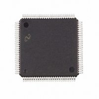
LM9832CCVJD National Semiconductor, LM9832CCVJD Datasheet - Page 5

LM9832CCVJD
Manufacturer Part Number
LM9832CCVJD
Description
IC SCANNER CLR USB IMAGE 100TQFP
Manufacturer
National Semiconductor
Datasheet
1.LM9832CCVJD.pdf
(42 pages)
Specifications of LM9832CCVJD
Number Of Bits
14
Number Of Channels
3
Voltage - Supply, Analog
5V
Voltage - Supply, Digital
5V
Package / Case
100-TQFP, 100-VQFP
Lead Free Status / RoHS Status
Contains lead / RoHS non-compliant
Power (watts)
-
Other names
*LM9832CCVJD
Available stocks
Company
Part Number
Manufacturer
Quantity
Price
Company:
Part Number:
LM9832CCVJD
Manufacturer:
Texas Instruments
Quantity:
10 000
Electrical Characteristics
The following specifications apply for AGND=DGND=0V, V
100%, unless otherwise noted. Boldface limits apply for T
Full Channel Characteristics (in units of 12 bit LSBs unless otherwise noted)
Coarse Color Balance PGA Characteristics (Configuration Registers 3B, 3C, and 3D)
Static Offset DAC Characteristics (Configuration Registers 38, 39, and 3A)
Absolute Maximum Ratings
Positive Supply Voltage (V
With Respect to GND=AGND=DGND
Voltage On Any Input or Output Pin
Input Current at any pin (Note 3)
Package Input Current (Note 3)
Package Dissipation at T
ESD Susceptibility (Note 5)
Soldering Information
Storage Temperature
Symbol
V
V
V
Human Body Model
Machine Model
Infrared, 10 seconds (Note 6)
DNL
INL
OS1
OS2
OS3
C
Resolution with No Missing Codes
Differential Non-Linearity
(Note 14)
Integral Non-Linearity Error
(Notes 11 & 14)
Analog Channel Gain Constant
(ADC Codes/V), referred to 14 bits.
Pre-Boost Analog Channel Offset Error
Pre-PGA Analog Channel Offset Error
Post-PGA Analog Channel Offset Error
Monotonicity
G
G
x3 Boost Gain
Gain Error at any gain (Note 13)
Monotonicity
Offset DAC LSB size
Offset DAC Adjustment Range
0
31
(Minimum PGA Gain)
(Maximum PGA Gain)
A
+
= 25°C
Parameter
=V
A
=V
D
=V
DRAM
)
-0.3V to V
-65°C to +150°
(Notes 1 & 2)
(Note 4)
±25mA
±50mA
2000 V
+
235°C
+0.3V
250 V
Bias Current = 80%,
V
Bias Current = 80%,
V
Includes voltage reference
variation, gain setting = 1
PGA Setting = 0
PGA Setting = 31
x3 Boost Setting On
(bit B5 of Gain Register is set)
PGA gain = 1
PGA gain = 1
6.5V
A
DRAM
DRAM
A
=V
=T
D
J
=V
=3.3V
=3.3V
=T
5
DRAM
MIN
Operating Ratings
Operating Temperature Range
LM9832CCVJD
V
V
V
|V
Input Voltage Range
Conditions
A
D
DRAM
A
to T
Supply Voltage
-V
Supply Voltage
=+5.0V
D
|
MAX
Supply Voltage
; all other limits T
DC
, f
CRYSTAL IN
= 48MHz, Analog Bias Current =
A
(Note 9)
Typical
=T
+0.75
-0.45
8192
±278
+1.7
0.93
3.00
2.94
-2.3
-30
-26
0.3
14
26
J
9
+2.85V ≤ V
=25°C. (Notes 8, 9, & 10)
(Notes 1 & 2)
(Note 10)
-0.05V to V
Limits
DRAM
7412
9300
±256
+2.4
+7.5
0.90
0.96
2.95
3.10
2.85
3.04
+0.9
-0.9
-8.5
-0.6
+76
+31
+26
-34
-80
-75
+4.75V to +5.25V
+4.75V to +5.25V
12
12
5
6
6
0°C≤T
www.national.com
T
≤ V
MIN
D
≤T
+
≤ 100mV
LSB (max)
LSB (max)
LSB (max)
A
+100mV
LSB (min)
LSB (min)
LSB (min)
V/V (max)
V/V (max)
V/V (max)
mV (max)
mV (max)
mV (max)
mV (max)
bits (min)
bits (min)
V/V (min)
V/V (min)
V/V (min)
bits (min)
+ 0.05V
mV (min)
mV (min)
mV (min)
mV (min)
mV (min)
≤+70°C
% (max)
(Limits)
% (min)
A
Units
≤T
MAX


