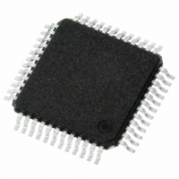
STLC7550TQF7TR STMicroelectronics, STLC7550TQF7TR Datasheet - Page 10

STLC7550TQF7TR
Manufacturer Part Number
STLC7550TQF7TR
Description
IC ANALOG FRONT END LV 48-TQFP
Manufacturer
STMicroelectronics
Datasheet
1.E-STLC7550TQF7.pdf
(24 pages)
Specifications of STLC7550TQF7TR
Number Of Bits
16
Number Of Channels
1
Power (watts)
30mW
Voltage - Supply, Analog
3V
Voltage - Supply, Digital
3V
Package / Case
48-TQFP, 48-VQFP
Lead Free Status / RoHS Status
Lead free / RoHS Compliant
Available stocks
Company
Part Number
Manufacturer
Quantity
Price
Company:
Part Number:
STLC7550TQF7TR
Manufacturer:
STMicroelectronics
Quantity:
10 000
Functional description
2.4
10/24
Modes of operation
Figure 3.
Thanks to MCM and M/S programmation pins we can get the following configuration.
Configuration 1 : MCM = 1, M/S = 1
The STLC7550 is in master mode and we have :
Fs = XTAL IN / (M x Q x OVER)
Fs and SCLK are output pins.
Figure 4.
Configuration 2 : MCM = 1, M/S = 0
The STLC7550 is in slave mode. SCLK is provided by the STLC7550, the processor
generates the Fs and controls the phase of the sampling frequency.
Fs must be the result of a division of a number of cycles of SLCK (Fs = SCLK % OVER).
Configuration 3 : MCM = 0, M/S = 1
The STLC7550 is in master mode and the processor provides the XTAL IN = MCLK =
OCLK. The STLC7550 generates the Fs from OCLK. In this mode the configuration 3 is
equivalent to the STLC7546 mode.
Configuration 4 : MCM = 0, M/S = 0
The STLC7550 is in slave mode. The configuration 4 is equivalent to configuration 3 but the
Fs is generated and phase controlled by the processor.
Clock Block Diagram
Configuration 1
XTALIN
(MCLK)
Cont. Reg. : Bit 8-9-10-11-12-13
V
DD
÷ M
PROCESSOR
XTALOUT
÷ Q
BCLK
DO
FS
DI
Rev 9
MCM
(OCLK)
SCLK
SCLK
FS
DIN
DOUT
f
Q
STLC7550
= 36.864MHz
XTALIN
% OVER
Bit 3-4-5
MCM
Sync
M/S
TS
M/S
V
V
GND
DD
DD
Internal
Sampling
FS
STLC7550


