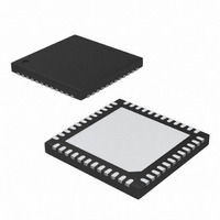
MAX5864ETM+ Maxim Integrated Products, MAX5864ETM+ Datasheet - Page 14

MAX5864ETM+
Manufacturer Part Number
MAX5864ETM+
Description
IC ANLG FRONT END 22MSPS 48-TQFN
Manufacturer
Maxim Integrated Products
Datasheet
1.MAX5864ETM.pdf
(26 pages)
Specifications of MAX5864ETM+
Number Of Bits
10
Number Of Channels
4
Power (watts)
2.10W
Voltage - Supply, Analog
2.7 V ~ 3.3 V
Voltage - Supply, Digital
1.8 V ~ 3.3 V
Package / Case
48-TQFN Exposed Pad
Lead Free Status / RoHS Status
Lead free / RoHS Compliant
The ADC uses a seven-stage, fully differential,
pipelined architecture that allows for high-speed con-
version while minimizing power consumption. Samples
taken at the inputs move progressively through the
pipeline stages every half-clock cycle. Including the
delay through the output latch, the total clock-cycle
latency is 5 clock cycles for channel IA and 5.5 clock
cycles for channel QA. The ADC’s full-scale analog
input range is ±V
of V
and V
for details.
Figure 1
ADC’s input T/H circuitry. In track mode, switches S1,
S2a, S2b, S4a, S4b, S5a, and S5b are closed. The fully
differential circuits sample the input signals onto the
two capacitors (C2a and C2b) through switches S4a
and S4b. S2a and S2b set the common mode for the
amplifier input, and open simultaneously with S1, sam-
pling the input waveform. Switches S4a, S4b, S5a, and
S5b are then opened before switches S3a and S3b
connect capacitors C1a and C1b to the output of the
amplifier and switch S4c is closed. The resulting differ-
ential voltages are held on capacitors C2a and C2b.
Ultra-Low-Power, High Dynamic-
Performance, 22Msps Analog Front End
Table 1. Output Codes vs. Input Voltage
14
DD
______________________________________________________________________________________
REFN
INPUT VOLTAGE
/2 ±0.2V. V
DIFFERENTIAL
−
−
−
displays a simplified functional diagram of the
V
V
V
V
V
V
V
REF
REF
REF
REF
REF
REF
REF
. See the Reference Configurations section
×
×
×
×
×
×
×
127
128
126
128
128
128
128
127
128
128
128
1
0
1
REF
REF
Input Track-and-Hold (T/H) Circuits
with a common-mode input range
is the difference between V
DIFFERENTIAL INPUT
(+full scale - 1LSB)
(+full scale - 2LSB)
(-full scale + 1LSB)
Dual 8-Bit ADC
(bipolar zero)
(-full scale)
(LSB)
-127
-128
127
126
+1
-1
0
REFP
The amplifiers charge capacitors C1a and C1b to the
same values originally held on C2a and C2b. These val-
ues are then presented to the first-stage quantizers and
isolate the pipelines from the fast-changing inputs. The
wide input bandwidth T/H amplifiers allow the ADC to
track and sample/hold analog inputs of high frequen-
cies (> Nyquist). Both ADC inputs (IA+, QA+, IA-, and
QA-) can be driven either differentially or single ended.
Match the impedance of IA+ and IA-, as well as QA+
and QA-, and set the common-mode voltage to mid-
supply (V
DA0–DA7 are the ADCs’ digital logic outputs. The logic
level is set by OV
put coding is offset binary
capacitive load on digital outputs DA0–DA7 should be
kept as low as possible (<15pF) to avoid large digital
currents feeding back into the analog portion of the
MAX5864 and degrading its dynamic performance.
Buffers on the digital outputs isolate them from heavy
capacitive loads. Adding 100Ω resistors in series with
the digital outputs close to the MAX5864 helps improve
ADC performance. Refer to the MAX5865 EV kit
schematic for an example of the digital outputs driving
a digital buffer through 100Ω series resistors.
OFFSET BINARY
(DA7–DA0)
1111 1111
1111 1110
1000 0001
1000 0000
0111 1111
0000 0001
0000 0000
DD
/2) for optimum performance.
ADC Digital Output Data (DA0–DA7)
DD
from 1.8V to V
(Table 1, Figure
OUTPUT DECIMAL
DD
CODE
. The digital out-
255
254
129
128
127
1
0
2). The


