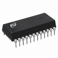
DP8572AN National Semiconductor, DP8572AN Datasheet - Page 16

DP8572AN
Manufacturer Part Number
DP8572AN
Description
IC REAL TIME CLOCK W/RAM 24 DIP
Manufacturer
National Semiconductor
Type
Clock/Calendar/NVSRAMr
Datasheet
1.DP8572AN.pdf
(22 pages)
Specifications of DP8572AN
Memory Size
44B
Time Format
HH:MM:SS:hh (12/24 hr)
Date Format
YY-MM-DD-dd
Interface
Parallel
Voltage - Supply
4.5 V ~ 5.5 V
Operating Temperature
-40°C ~ 85°C
Mounting Type
Through Hole
Package / Case
24-DIP (0.300", 7.62mm)
Lead Free Status / RoHS Status
Contains lead / RoHS non-compliant
Other names
*DP8572AN
DP8572
DP8572
Available stocks
Company
Part Number
Manufacturer
Quantity
Price
Part Number:
DP8572AN
Manufacturer:
TOSHIBA/东芝
Quantity:
20 000
Functional Description
D5 The Delay Enable bit is used when a power fail occurs
If this bit is set a 480 s delay is generated internally before
the
access the registers for up to 480
power fail interrupt After a power failure is detected but
prior to the 480 s delay timing out the host P may force
immediate lock out by resetting the Delay Enable bit Note if
this bit is a 0 when power fails then after a delay of 30 s
min 63 s max the P cannot read the chip
D6 This read only bit is set and reset by the voltage at the
V
battery voltage at the V
tor monitors the battery and when the voltage is lower than
2 1V (typical) this bit is set The power fail interrupt must be
enabled to check for a low battery voltage
D7 Time Save Enable bit controls the loading of real-time-
clock data into the Time Save RAM When a one is written
to this bit the Time Save RAM will follow the corresponding
clock registers and when a zero is written to this bit the time
in the Time Save RAM is frozen This eliminates any syn-
chronization problems when reading the clock thus negat-
ing the need to check for a counter rollover during a read
cycle
This bit must be set to a one prior to power failing to enable
the Time Save feature When the power fails this bit is auto-
matically reset and the time is saved in the Time Save RAM
REAL TIME MODE REGISTER
D0–D1 These are the leap year counter bits These bits are
written to set the number of years from the previous leap
year The leap year counter increments on December 31st
and it internally enables the February 29th counter state
This method of setting the leap year allows leap year to
occur whenever the user wishes to thus providing flexibility
in implementing Japanese leap year function
BB
LY1
pin It can be used by the P to determine whether the
P interface is locked out This will enable the
0
0
1
1
LY0
0
1
0
1
BB
pin is getting too low A compara-
Leap Year Current Year
Leap Year Last Year
Leap Year 2 Years Ago
Leap Year 3 Years Ago
Leap Year
s after it receives a
(Continued)
Counter
TL F 9980– 15
P to
16
D2 The count mode for the hours counter can be set to
either 24 hour mode or 12 hour mode with AM PM indicator
A one will place the clock in 12 hour mode
D3 This bit is the master Start Stop bit for the clock When
a one is written to this bit the real time counter’s prescaler
and counter chain are enabled When this bit is reset to zero
the contents of the real time counter is stopped and the
prescaler is cleared When the RTC is initially powered up
this bit will be held at a logic 0 until the oscillator starts
functioning correctly after which this bit may be modified If
an oscillator fail event occurs this bit will be reset to logic 0
D4 This bit controls the operation of the interrupt output in
standby mode If set to a one it allows Alarm Periodic and
Power Fail interrupts to be functional in standby mode Note
that the MFO pin is configured as open drain in standby
mode
If bit D4 is set to a zero then bits D0 – D5 of Interrupt Control
Register 0 and bits D6 and D7 of Interrupt Control Register
1 will be reset when the RTC enters the standby mode
(V
tem (V
D5 General purpose RAM
D6 and D7 These two bits select the crystal clock frequen-
cy as per the following table
All bits are Read Write and any mode written into this regis-
ter can be determined by reading the register On initial
power up these bits are random
OUTPUT MODE REGISTER
BB l
CC
V
) power is restored
CC
) They will have to be re-configured when sys-
XT1
D0– D6 General Purpose RAM
0
0
1
1
XT0
0
1
0
1
32 768 kHz
4 194304 MHz
4 9152 MHz
32 000 kHz
Frequency
Crystal
TL F 9980– 16


