DS1746P-70+ Maxim Integrated Products, DS1746P-70+ Datasheet
DS1746P-70+
Specifications of DS1746P-70+


Related parts for DS1746P-70+


DS1746P-70+ Summary of contents
Page 1
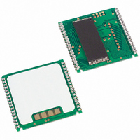
... V CC A16 Maxim 31 A15 2 DS1746 A14 N. A12 A13 A11 A10 DQ7 DQ6 DQ0 14 19 DQ1 DQ5 DQ2 15 18 DQ4 17 GND 16 DQ3 Encapsulated DIP 34 1 Maxim DS1746P GND BAT PowerCap Module Board (Uses DS9034PCX PowerCap N.C. N.C. A14 A13 A12 A11 A10 ...
Page 2
... V CC RST — 4 X1, X2, — V BAT DS1746/DS1746P Y2K-Compliant, Nonvolatile Timekeeping RAMs FUNCTION No Connection Address Input Data Input/Output Ground Active-Low Chip Enable Input Active-Low Output Enable Input Active-Low Write-Enable Input Power-Supply Input Active-Low Power-Fail Output, Open Drain. Requires a pullup resistor for proper operation. ...
Page 3
... ORDERING INFORMATION VOLTAGE PART RANGE (V) DS1746-70+ 5.0 DS1746-70IND+ 5.0 DS1746P-70+ 5.0 DS1746P-70IND+ 5.0 DS1746W-120+ 3.3 DS1746W-120IND+ 3.3 DS1746WP-120+ 3.3 DS1746WP-120IND+ 3.3 +Denotes a lead(Pb)-free/RoHS-compliant package. The top mark will include a “+” symbol on lead-free devices. *DS9034-PCX+ or DS9034I-PCX+ required (must be ordered separately). ...
Page 4
... This design allows the PowerCap to be mounted on top of the DS1746P after the completion of the surface mount process. Mounting the PowerCap after the surface mount process prevents damage to the crystal and battery due to the high temperatures required for solder reflow ...
Page 5
... The electrical environment also affects clock accuracy and caution should be taken to place the RTC in the lowest-level EMI section of the PC board layout. For additional information, refer to Application Note 58. DS1746/DS1746P Y2K-Compliant, Nonvolatile Timekeeping RAMs OE WE MODE ...
Page 6
... low prior to WE transitioning low the data bus can become active with read data defined by the address inputs. A low transition on WE will after WE goes active. then disable the output t WEZ DS1746/DS1746P Y2K-Compliant, Nonvolatile Timekeeping RAMs DATA ...
Page 7
... This bit is not writable and should always be a one when read zero is ever present, an exhausted lithium energy source is indicated and both the contents of the RTC and RAM are questionable. DS1746/DS1746P Y2K-Compliant, Nonvolatile Timekeeping RAMs , (point at which write protection occurs) the PF ...
Page 8
... Output Leakage Current (any output) Output Logic 1 Voltage (I = -1.0 mA) OUT Output Logic 0 Voltage (I = +2.1 mA) OUT Write Protection Voltage Battery Switchover Voltage DS1746/DS1746P Y2K-Compliant, Nonvolatile Timekeeping RAMs TEMP RANGE 0°C to +70°C, Noncondensing -40°C to +85°C, Noncondensing SYMBOL MIN TYP V 2 2.0 ...
Page 9
... AC CHARACTERISTICS—READ CYCLE (5V) = 5.0V 10 Over the Operating Range PARAMETER Read Cycle Time Address Access Time Low-Z CE Access Time CE Data Off Time Low-Z OE Access Time OE Data Off Time Output Hold from Address DS1746/DS1746P Y2K-Compliant, Nonvolatile Timekeeping RAMs SYMBOL MIN TYP Icc Icc 1 Icc ...
Page 10
... Address Access Time Low-Z CE Access Time CE Data Off Time Low-Z OE Access Time OE Data Off Time Output Hold from Address READ CYCLE TIMING DIAGRAM A0-A16 CEA CE t CEL OE DQ0-DQ7 DS1746/DS1746P Y2K-Compliant, Nonvolatile Timekeeping RAMs SYMBOL MIN t 120 CEL t CEA t CEZ t 5 OEL t ...
Page 11
... PARAMETER Write Cycle Time Address Setup Time WE Pulse Width CE Pulse Width CE and CE2 Pulse Width Data Setup Time Data Hold Time Data Hold Time WE Data Off Time Write Recovery Time Write Recovery Time DS1746/DS1746P Y2K-Compliant, Nonvolatile Timekeeping RAMs SYMBOL MIN TYP ...
Page 12
... WRITE CYCLE TIMING DIAGRAM, WRITE-ENABLE CONTROLLED A0-A16 WEZ DQ0-DQ7 DATA OUTPUT WRITE CYCLE TIMING DIAGRAM, CHIP-ENABLE CONTROLLED A0-A16 DQ0-DQ7 DS1746/DS1746P Y2K-Compliant, Nonvolatile Timekeeping RAMs VALID t t WEW WR1 DH1 DATA INPUT t WC VALID t t CEW WR2 DH2 DATA INPUT ...
Page 13
... PARAMETER Before Power-Down V Fall Time PF(MAX) V PF(MIN) V Fall Time PF(MIN Rise Time PF(MIN) V PF(MAX) Power-Up Recover Time Expected Data-Retention Time (Oscillator ON) POWER-UP/DOWN TIMING (5V DEVICE) DS1746/DS1746P Y2K-Compliant, Nonvolatile Timekeeping RAMs SYMBOL MIN TYP 300 REC MAX UNITS NOTES s s s s ...
Page 14
... PF(MIN) V Rise Time PF(MIN) V PF(MAX RST High PF Expected Data-Retention Time (Oscillator ON) POWER-UP/DOWN WAVEFORM TIMING (3.3V DEVICE) CAPACITANCE (T = +25°C) A PARAMETER Capacitance on All Input Pins Capacitance on All Output Pins DS1746/DS1746P Y2K-Compliant, Nonvolatile Timekeeping RAMs SYMBOL MIN TYP 300 REC SYMBOL MIN TYP ...
Page 15
... RoHS status only. Package drawings may show a different suffix character, but the drawing pertains to the package regardless of RoHS status. PACKAGE TYPE 32 EDIP 34 PWRCP DS1746/DS1746P Y2K-Compliant, Nonvolatile Timekeeping RAMs starting from the time power is first applied by the user. PACKAGE CODE DOCUMENT NO. MDF32+1 ...
Page 16
... Maxim cannot assume responsibility for use of any circuitry other than circuitry entirely embodied in a Maxim product. No circuit patent licenses are implied. Maxim reserves the right to change the circuitry and specifications without notice at any time 2010 Maxim Integrated Products DS1746/DS1746P Y2K-Compliant, Nonvolatile Timekeeping RAMs DESCRIPTION as specified by RAM vendors Maxim and the Dallas logo are registered trademarks of Maxim Integrated Products ...