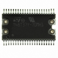
M48T37Y-70MH1E STMicroelectronics, M48T37Y-70MH1E Datasheet - Page 7

M48T37Y-70MH1E
Manufacturer Part Number
M48T37Y-70MH1E
Description
IC TIMEKPR NVRAM 256KBIT5V 44SOH
Manufacturer
STMicroelectronics
Series
Timekeeper®r
Type
Clock/Calendar/NVSRAMr
Specifications of M48T37Y-70MH1E
Memory Size
256K (32K x 8)
Time Format
HH:MM:SS (24 hr)
Date Format
YY-MM-DD-dd
Interface
Parallel
Voltage - Supply
4.5 V ~ 5.5 V
Operating Temperature
0°C ~ 70°C
Mounting Type
Surface Mount
Package / Case
44-SOH
Bus Type
Parallel
User Ram
32KB
Operating Supply Voltage (typ)
5V
Package Type
SOH
Operating Supply Voltage (max)
5.5V
Operating Supply Voltage (min)
4.5V
Operating Temperature Classification
Commercial
Operating Temperature (max)
70C
Operating Temperature (min)
0C
Pin Count
44
Mounting
Surface Mount
Memory Configuration
32K X 8
Nvram Features
RTC
Interface Type
Parallel
Access Time
70ns
Supply Voltage Range
4.5V To 5.5V
Memory Case Style
SOIC
No. Of Pins
44
Rohs Compliant
Yes
Lead Free Status / RoHS Status
Lead free / RoHS Compliant
Other names
497-2854-5
M48T37Y-70MH1
M48T37Y-70MH1
Available stocks
Company
Part Number
Manufacturer
Quantity
Price
Company:
Part Number:
M48T37Y-70MH1E
Manufacturer:
ST
Quantity:
936
OPERATION MODES
As
ray and the quartz controlled clock oscillator of the
M48T37Y/V are integrated on one silicon chip.
The memory locations that provide user accessi-
ble BYTEWIDE™ clock information are in the
bytes with addresses 7FF1 and 7FF9h-7FFFh (lo-
cated in
contain the century, year, month, date, day, hour,
minute, and second in 24 hour BCD format. Cor-
rections for 28, 29 (leap year - valid until the year
2100), 30, and 31 day months are made automat-
ically.
Byte 7FF8h is the clock control register. This byte
controls user access to the clock information and
also stores the clock calibration setting.
Byte 7FF7h contains the watchdog timer setting.
The watchdog timer redirects an out-of-control mi-
croprocessor and provides a reset or interrupt to it.
Bytes 7FF2h-7FF5h are reserved for clock alarm
programming. These bytes can be used to set the
alarm. This will generate an active low signal on
Table 2. Operating Modes
Note: X = V
Deselect
WRITE
READ
READ
Deselect
Deselect
Figure 4., page 6
Mode
1. See
IH
Table 5., page
Table 13., page 23
or V
IL
; V
SO
V
SO
= Battery Back-up Switchover Voltage.
shows, the static memory ar-
4.5 to 5.5V
3.0 to 3.6V
to V
V
13). The clock locations
V
PFD
for details.
or
SO
CC
(1)
(min)
(1)
V
V
V
V
E
X
X
IH
IL
IL
IL
V
V
G
X
X
X
X
the IRQ/FT pin when the alarm bytes match the
date, hours, minutes, and seconds of the clock.
The eight clock bytes are not the actual clock
counters themselves; they are memory locations
consisting of BiPORT™ READ/WRITE memory
cells. The M48T37Y/V includes a clock control cir-
cuit which updates the clock bytes with current in-
formation once per second. The information can
be accessed by the user in the same manner as
any other location in the static memory array.
The M48T37Y/V also has its own Power-fail De-
tect circuit. The control circuitry constantly moni-
tors the single V
condition. When V
write protects the SRAM, providing a high degree
of data security in the midst of unpredictable sys-
tem operation brought on by low V
below the Battery Back-up Switchover Voltage
(V
which maintains data and clock operation until val-
id power returns.
IH
IL
SO
), the control circuitry connects the battery
V
V
V
W
X
X
X
IH
IH
IL
CC
DQ0-DQ7
High Z
High Z
High Z
High Z
CC
D
D
supply for an out of tolerance
OUT
IN
is out of tolerance, the circuit
M48T37Y, M48T37V
Battery Back-up Mode
CMOS Standby
CC
Standby
Power
Active
Active
Active
. As V
CC
falls
7/29


