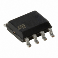
M41T00M6E STMicroelectronics, M41T00M6E Datasheet - Page 9

M41T00M6E
Manufacturer Part Number
M41T00M6E
Description
IC RTC SERIAL 8SOIC
Manufacturer
STMicroelectronics
Type
Clock/Calendar/NVSRAMr
Specifications of M41T00M6E
Memory Size
8B
Time Format
HH:MM:SS (24 hr)
Date Format
YY-MM-DD-dd
Interface
I²C, 2-Wire Serial
Voltage - Supply
2 V ~ 5.5 V
Operating Temperature
-40°C ~ 85°C
Mounting Type
Surface Mount
Package / Case
8-SOIC (3.9mm Width)
Function
Clock/Calendar/Battery Backup
Rtc Memory Size
8 Byte
Supply Voltage (max)
5.5 V
Supply Voltage (min)
2 V
Maximum Operating Temperature
+ 85 C
Minimum Operating Temperature
- 40 C
Mounting Style
SMD/SMT
Rtc Bus Interface
Serial (2-Wire, I2C)
Nvram Features
RTC, Internal Battery, XTAL
Interface Type
I2C, Serial
Supply Voltage Range
2V To 5.5V
Memory Case Style
SOIC
No. Of Pins
8
Operating Temperature Range
-40°C To
Rohs Compliant
Yes
Lead Free Status / RoHS Status
Contains lead / RoHS non-compliant
Other names
497-2810-5
M41T00M6
M41T00M6
Available stocks
Company
Part Number
Manufacturer
Quantity
Price
Company:
Part Number:
M41T00M6E
Manufacturer:
AVAGO
Quantity:
1 000
Part Number:
M41T00M6E
Manufacturer:
ST
Quantity:
20 000
READ Mode
In this mode, the master reads the M41T00 slave
after setting the slave address (see Figure 8). Fol-
lowing the WRITE Mode Control Bit (R/W = 0) and
the Acknowledge Bit, the word address An is writ-
ten to the on-chip address pointer. Next the
START condition and slave address are repeated,
followed by the READ Mode Control Bit (R/W = 1).
At this point, the master transmitter becomes the
master receiver. The data byte which was ad-
dressed will be transmitted and the master receiv-
er will send an Acknowledge Bit to the slave
transmitter. The address pointer is only increment-
ed on reception of an Acknowledge Bit. The
Figure 8. Slave Address Location
Figure 9. READ Mode Sequence
BUS ACTIVITY:
MASTER
SDA LINE
BUS ACTIVITY:
S
ADDRESS
SLAVE
DATA n+X
START
ADDRESS (An)
WORD
P
1
1
SLAVE ADDRESS
S
0
ADDRESS
1
SLAVE
M41T00 slave transmitter will now place the data
byte at address A
ceiver reads and acknowledges the new byte and
the address pointer is incremented to A
This cycle of reading consecutive addresses will
continue until the master receiver sends a STOP
condition to the slave transmitter.
An alternate READ Mode may also be implement-
ed, whereby the master reads the M41T00 slave
without first writing to the (volatile) address point-
er. The first address that is read is the last one
stored in the pointer (see
0
0
0
R/W
A
DATA n
AI00602
n+1
on the bus. The master re-
Figure 10., page
DATA n+1
AI00899
n+2
M41T00
.
10).
9/21


