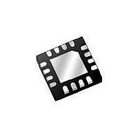
PCF2123BS/1,512 NXP Semiconductors, PCF2123BS/1,512 Datasheet - Page 5

PCF2123BS/1,512
Manufacturer Part Number
PCF2123BS/1,512
Description
IC CLOCK HVQFN16
Manufacturer
NXP Semiconductors
Type
Clock/Calendar/Alarmr
Datasheet
1.PCF2123TS1118.pdf
(61 pages)
Specifications of PCF2123BS/1,512
Package / Case
16-VQFN Exposed Pad, 16-HVQFN, 16-SQFN, 16-DHVQFN
Time Format
HH:MM:SS (12/24 hr)
Date Format
YY-MM-DD-dd
Interface
SPI, 3-Wire Serial
Voltage - Supply
1.1 V ~ 5.5 V
Operating Temperature
-40°C ~ 85°C
Mounting Type
Surface Mount
Function
Clock, Calendar, Alarm, Watchdog
Supply Voltage (max)
5.5 V
Supply Voltage (min)
1.1 V
Maximum Operating Temperature
+ 85 C
Minimum Operating Temperature
- 40 C
Mounting Style
SMD/SMT
Rtc Bus Interface
SPI
Supply Current
250 uA
Lead Free Status / RoHS Status
Lead free / RoHS Compliant
Memory Size
-
Lead Free Status / RoHS Status
Lead free / RoHS Compliant, Lead free / RoHS Compliant
Other names
568-5051-5
935286382512
935286382512
NXP Semiconductors
Table 3.
[1]
[2]
PCF2123
Product data sheet
Symbol
OSCI
OSCO
n.c.
TEST
INT
CE
V
SDO
SDI
SCL
CLKOE
CLKOUT 13
V
SS
DD
The die paddle (exposed pad) is wired to V
The substrate (rear side of the die) is wired to V
Pin
TSSOP14
(PCF2123TS/1)
1
2
3, 11
4
5
6
7
8
9
10
12
14
Pin description
7.2 Pin description
HVQFN16
(PCF2123BS/1)
16
1
6, 7, 14, 15
2
3
4
5
8
9
10
11
12
13
[1]
All information provided in this document is subject to legal disclaimers.
SS
and should be electrically isolated.
SS
PCF2123Ux
(bare die)
7
8
-
9
10
11
12
1
2
3
5
4
6
Rev. 4 — 22 December 2010
and should be electrically isolated.
[2]
oscillator input; high-impedance node; minimize wire length
oscillator output; high-impedance node; minimize wire
do not connect and do not use as feed through; connect to
test pin; not user accessible; connect to V
serial data output, push-pull; high-impedance when not
serial data input; may float when CE is inactive
serial clock input; may float when CE is inactive
clock output (open-drain)
Description
between quartz and package
length between quartz and package
V
(internally pulled down)
interrupt output (open-drain; active LOW)
chip enable input (active HIGH) with internal pull down
ground
driving; can be connected to SDI for single wire data line
CLKOUT enable or disable pin; enable is active HIGH
supply voltage; positive or negative steps in V
oscillator performance; recommend 100 nF decoupling
close to device (see
DD
if floating pins are not allowed
Figure
SPI Real time clock/calendar
29)
PCF2123
© NXP B.V. 2010. All rights reserved.
SS
or leave floating
DD
may affect
5 of 61


