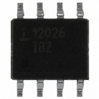
ISL12026IBZ Intersil, ISL12026IBZ Datasheet - Page 15

ISL12026IBZ
Manufacturer Part Number
ISL12026IBZ
Description
IC RTC/CALENDAR EEPROM 8-SOIC
Manufacturer
Intersil
Type
Clock/Calendar/EEPROMr
Specifications of ISL12026IBZ
Memory Size
4K (512 x 8)
Time Format
HH:MM:SS (12/24 hr)
Date Format
YY-MM-DD-dd
Interface
I²C, 2-Wire Serial
Voltage - Supply
2.7 V ~ 5.5 V
Operating Temperature
-40°C ~ 85°C
Mounting Type
Surface Mount
Package / Case
8-SOIC (3.9mm Width)
Clock Format
HH
Clock Ic Type
RTC
Interface Type
I2C, Serial
Memory Configuration
512 X 8
Supply Voltage Range
2.7V To 5.5V
Digital Ic Case Style
SOIC
Rohs Compliant
Yes
Lead Free Status / RoHS Status
Lead free / RoHS Compliant
Available stocks
Company
Part Number
Manufacturer
Quantity
Price
Company:
Part Number:
ISL12026IBZ
Manufacturer:
INTELSEL
Quantity:
60
Part Number:
ISL12026IBZ
Manufacturer:
INTERSIL
Quantity:
20 000
Part Number:
ISL12026IBZ-T
Manufacturer:
INTERSIL
Quantity:
20 000
Device Addressing
Following a start condition, the master must output a Slave
Address Byte. The first four bits of the Slave Address Byte
specify access to either the EEPROM array or to the CCR.
Slave bits ‘1010’ access the EEPROM array. Slave bits
‘1101’ access the CCR.
When shipped from the factory, EEPROM array is
UNDEFINED, and should be programmed by the customer
to a known state.
Bit 3 through Bit 1 of the slave byte specify the device select
bits. These are set to ‘111’.
The last bit of the Slave Address Byte defines the operation
to be performed. When this R/W bit is a one, then a read
operation is selected. A zero selects a write operation (Refer
to Figure 15).
After loading the entire Slave Address Byte from the SDA
bus, the ISL12026 compares the device identifier and device
FROM TRANSMITTER
DATA OUTPUT
FROM RECEIVER
DATA OUTPUT
SCL FROM
MASTER
SDA
SCL
SDA
SCL
15
FIGURE 14. ACKNOWLEDGE RESPONSE FROM RECEIVER
START
FIGURE 12. VALID DATA CHANGES ON THE SDA BUS
FIGURE 13. VALID START AND STOP CONDITIONS
DATA STABLE
START
1
ISL12026
DATA CHANGE
select bits with ‘1010111’ or ‘1101111’. Upon a correct
compare, the device outputs an acknowledge on the SDA
line.
Following the Slave Byte is a two byte word address. The
word address is either supplied by the master device or
obtained from an internal counter. On power up the internal
address counter is set to address 0h, so a current address
read of the EEPROM array starts at address 0. When
required, as part of a random read, the master must supply
the 2 Word Address Bytes as shown in Figure 15.
In a random read operation, the slave byte in the “dummy
write” portion must match the slave byte in the “read”
section. That is if the random read is from the array the slave
byte must be 1010111x in both instances. Similarly, for a
random read of the Clock/Control Registers, the slave byte
must be 1101111x in both places.
DATA STABLE
8
STOP
ACKNOWLEDGE
9
October 23, 2006
FN8231.5


