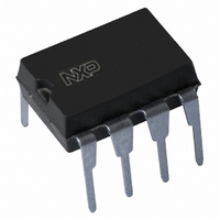
PCF8593P,112 NXP Semiconductors, PCF8593P,112 Datasheet - Page 16

PCF8593P,112
Manufacturer Part Number
PCF8593P,112
Description
IC CLOCK/CALENDAR LOW PWR 8-DIP
Manufacturer
NXP Semiconductors
Type
Clock/Calendar/NVSRAMr
Datasheet
1.PCF8593T1118.pdf
(35 pages)
Specifications of PCF8593P,112
Package / Case
8-DIP (0.300", 7.62mm)
Time Format
HH:MM:SS:hh (12/24 hr)
Date Format
YY-MM-DD-dd
Memory Size
8B
Interface
I²C, 2-Wire Serial
Voltage - Supply
1 V ~ 6 V
Operating Temperature
-40°C ~ 85°C
Mounting Type
Through Hole
Function
Clock/Calendar/Alarm/Timer Interrupt
Rtc Memory Size
8 Byte
Supply Voltage (max)
6 V
Supply Voltage (min)
1 V
Maximum Operating Temperature
+ 85 C
Minimum Operating Temperature
- 40 C
Mounting Style
Through Hole
Rtc Bus Interface
Serial (I2C)
Bus Type
Serial (I2C)
User Ram
8Byte
Package Type
PDIP
Operating Supply Voltage (max)
6V
Operating Temperature Classification
Industrial
Operating Temperature (max)
85C
Operating Temperature (min)
-40C
Pin Count
8
Mounting
Through Hole
Lead Free Status / RoHS Status
Lead free / RoHS Compliant
Lead Free Status / RoHS Status
Lead free / RoHS Compliant, Lead free / RoHS Compliant
Other names
568-1089-5
935151750112
PCF8593N
935151750112
PCF8593N
NXP Semiconductors
PCF8593
Product data sheet
8.2.1 Addressing
8.2.2 Clock and calendar READ or WRITE cycles
8.2 I
Before any data is transmitted on the I
addressed first. The addressing is always carried out with the first byte transmitted after
the start procedure.
The clock and calendar acts as a slave receiver or slave transmitter. The clock signal SCL
is only an input signal but the data signal SDA is a bidirectional line.
The clock and calendar slave address is shown in
Table 5.
The I
Figure
Bit
2
Fig 18. Master transmits to slave receiver (WRITE mode)
C-bus protocol
2
C-bus configuration for the different PCF8593 READ and WRITE cycles is shown in
18,
Slave address
7
MSB
1
Figure 19
S
I
2
C slave address byte
SLAVE ADDRESS
All information provided in this document is subject to legal disclaimers.
6
0
and
Rev. 04 — 6 October 2010
Figure
acknowledgement
R/W
from slave
0 A
5
1
20.
REGISTER ADDRESS A
2
C-bus, the device which must respond is
4
0
acknowledgement
from slave
3
0
Table
5.
Low power clock and calendar
n bytes
2
0
DATA
memory register address
auto increment
acknowledgement
from slave
1
1
PCF8593
© NXP B.V. 2010. All rights reserved.
A
013aaa346
P
0
LSB
R/W
16 of 35


