DS4100HW+ Maxim Integrated Products, DS4100HW+ Datasheet - Page 5
DS4100HW+
Manufacturer Part Number
DS4100HW+
Description
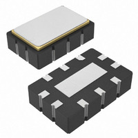
IC OSC CLOCK 100MHZ HCSL 10LCCC
Manufacturer
Maxim Integrated Products
Type
Clock Oscillatorr
Datasheet
1.DS4100H.pdf
(7 pages)
Specifications of DS4100HW+
Frequency
100MHz
Voltage - Supply
3.135 V ~ 3.465 V
Current - Supply
71mA
Operating Temperature
-40°C ~ 85°C
Package / Case
10-LCCC
Lead Free Status / RoHS Status
Lead free / RoHS Compliant
Count
-


Figure 2. Typical Termination for HCSL Driver and Test Conditions
Figure 3. HCSL Output Timing Diagram When OE is Enabled and Disabled
7–10
PIN
—
1
2
3
4
5
6
NAME
OUTN
RREF
OUTP
GND
N.C.
V
OE
_______________________________________________________________________________________
EP
CC
R
CL = SIMULATES RECEIVER INPUT CAPACITANCE FOR TEST ONLY.
OUTPUT
BUFFER
S
= 0Ω FOR TEST, 0 TO 33Ω TO MINIMIZE RINGING IN APPLICATION.
OUTP
OUTN
Output Enable. On-chip pullup resistor. If connected to logic-high or left open, the clock output is
enabled. If connected to logic-low, the output is three-stated.
Connect a 475
Ground
Positive Clock Output. Requires a series resistor and a pulldown resistor.
Negative Clock Output. Requires a series resistor and a pulldown resister.
+3.3V Supply Input. Device power can range from 3.135V to 3.465V.
No Connection
Exposed Paddle. Do not connect this pad or place exposed metal under the pad.
R
R
OUTN
OUTP
S
S
OE
GND
GND
0.7 x V
100MHz HCSL Clock Oscillator
±1% resistor from RREF to ground.
CC
R
t
t
T
PZH
PZL
R
T
R
T
= 50Ω
Z0 = 50Ω, 35in LENGTH
Z0
Z0
FUNCTION
OUTP
OUTN
t
PZ
0.3 x V
CC
CL
CL
CL = 2pF
RECEIVER
Pin Description
5
Related parts for DS4100HW+
Image
Part Number
Description
Manufacturer
Datasheet
Request
R

Part Number:
Description:
IC OSC CLOCK 250MHZ 10-LCCC
Manufacturer:
Maxim Integrated Products
Datasheet:
Part Number:
Description:
IC OSC CLOCK 150MHZ 10-LCCC
Manufacturer:
Maxim Integrated Products
Datasheet:
Part Number:
Description:
IC OSC CLOCK 160MHZ 10-LCCC
Manufacturer:
Maxim Integrated Products
Datasheet:
Part Number:
Description:
IC OSC CLOCK 160MHZ 10-LCCC
Manufacturer:
Maxim Integrated Products
Datasheet:
Part Number:
Description:
IC OSC CLOCK 155.52MHZ 10-LCCC
Manufacturer:
Maxim Integrated Products
Datasheet:
Part Number:
Description:
IC OSC CLOCK 156.25MHZ 10-LCCC
Manufacturer:
Maxim Integrated Products
Datasheet:
Part Number:
Description:
IC OSC CLOCK 125MHZ 10-LCCC
Manufacturer:
Maxim Integrated Products
Datasheet:
Part Number:
Description:
IC OSC CLOCK 155.52MHZ 10-LCCC
Manufacturer:
Maxim Integrated Products
Datasheet:
Part Number:
Description:
IC OSC CLOCK 156.25MHZ 10-LCCC
Manufacturer:
Maxim Integrated Products
Datasheet:
Part Number:
Description:
IC OSC CLOCK 150MHZ 10-LCCC
Manufacturer:
Maxim Integrated Products
Datasheet:
Part Number:
Description:
IC OSC CLOCK 300MHZ 10-LCCC
Manufacturer:
Maxim Integrated Products
Datasheet:
Part Number:
Description:
IC OSC CLOCK 300MHZ 10-LCCC
Manufacturer:
Maxim Integrated Products
Datasheet:
Part Number:
Description:
IC OSC CLOCK 250MHZ 10-LCCC
Manufacturer:
Maxim Integrated Products
Datasheet:

Part Number:
Description:
MAX7528KCWPMaxim Integrated Products [CMOS Dual 8-Bit Buffered Multiplying DACs]
Manufacturer:
Maxim Integrated Products
Datasheet:
Part Number:
Description:
Single +5V, fully integrated, 1.25Gbps laser diode driver.
Manufacturer:
Maxim Integrated Products
Datasheet: