DS4100HW+ Maxim Integrated Products, DS4100HW+ Datasheet - Page 3
DS4100HW+
Manufacturer Part Number
DS4100HW+
Description
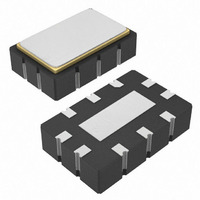
IC OSC CLOCK 100MHZ HCSL 10LCCC
Manufacturer
Maxim Integrated Products
Type
Clock Oscillatorr
Datasheet
1.DS4100H.pdf
(7 pages)
Specifications of DS4100HW+
Frequency
100MHz
Voltage - Supply
3.135 V ~ 3.465 V
Current - Supply
71mA
Operating Temperature
-40°C ~ 85°C
Package / Case
10-LCCC
Lead Free Status / RoHS Status
Lead free / RoHS Compliant
Count
-


ELECTRICAL CHARACTERISTICS (continued)
(V
Note 1: All voltages are referenced to ground.
Note 2: With 50Ω load to ground on each output pin.
Note 3: Guaranteed by design and not production tested.
Note 4: t
Note 5: t
Note 6: t
Note 7: Frequency stability is calculated as: Δf
Note 8: Measured with 50mV
Note 9: Including oscillator startup time and PLL acquisition time measured after V
Output Disable Time
CLOCK OUTPUT AS MEASURED AT OUTP WITH RESPECT TO OUTN
Clock Output
Frequency Stability
Total
Initial Frequency
Tolerance
Frequency Stability
vs. Temperature
Frequency Stability
vs. V
Frequency Stability
vs. Load
Aging (10 Years)
Phase Jitter (RMS)
Accumulated
Deterministic Jitter Due
to Power-Supply Noise
(Note 8)
Rise and Fall Time
Mismatching
Duty Cycle
Oscillation Startup Time
Clock Output SSB
Phase Noise
CC
= 3.135V to 3.465V, T
CC
PARAMETER
the falling edge of OUTP or OUTN.
V
less than 0.1V
PZL
PZH
PZ
OUTN
is defined as the time at which VOE = 1.0V on the falling edge of OE to the time at which both V
is defined as the time at which VOE = 1.0V on the rising edge of OE to the time at which V
is defined as the time at which the voltage on the rising edge of OE is equal to 1.0V to the time at which V
= 0.9V
_______________________________________________________________________________________
OH
OH
.
on the rising edge of V
A
SYMBOL
DJ
f / f
f
| LOAD
PJ
= -40°C to +85°C. Typical values are at V
f / f
AGING
f
f
P-P
_TOL
PN,P-P
t
OUT
f / f
f / f
t
DC
PZ
RMS
O
O
sinusoidal signal on the supply from 10kHz to 1MHz.
O
| T
O
| V V
A
Figure 3 (Note 6)
Over temperature range, aging, load, and supply (Note 7)
V
V
±10% variation in termination resistance
12kHz to 20MHz
10kHz
100kHz
200kHz
1MHz
20% to 80%; CL = 2pF; Figure 2;
2 x (t
Measure at OUTP and OUTN, Figure 2
(Note 9)
100Hz
1kHz
10kHz
100kHz
1MHz
10MHz
CC
CC
CC
= 3.3V, T
= 3.3V
= 3.3V ±5%
R
- t
TOTAL
100MHz HCSL Clock Oscillator
F
) / (t
OUTP
A
R
= Δf
= +25°C
+ t
or V
F
TEMP
)
OUTN
CONDITIONS
+ Δf
.
VCC
CC
x 0.165 + Δf
= +3.3V and T
CC
LOAD
reaches 3.0V from power-on.
A
= +25°C, unless otherwise noted.)
+ Δf
AGING
.
OUTP
MIN
-39
-30
45
-3
-7
OUTP
or V
-90.0
TYP
-112
-115
-123
-142
-147
100
±15
±20
0.9
3.0
7.0
±1
27
15
3
OUTN
and V
MAX UNITS
+39
+30
= 0.1V
OUTP
OUTN
+3
+7
10
55
or
are
OH
ppm/V
MHz
ppm
ppm
ppm
ppm
dBc/
ppm
ms
Hz
ns
ps
ps
%
%
on
3
Related parts for DS4100HW+
Image
Part Number
Description
Manufacturer
Datasheet
Request
R

Part Number:
Description:
IC OSC CLOCK 250MHZ 10-LCCC
Manufacturer:
Maxim Integrated Products
Datasheet:
Part Number:
Description:
IC OSC CLOCK 150MHZ 10-LCCC
Manufacturer:
Maxim Integrated Products
Datasheet:
Part Number:
Description:
IC OSC CLOCK 160MHZ 10-LCCC
Manufacturer:
Maxim Integrated Products
Datasheet:
Part Number:
Description:
IC OSC CLOCK 160MHZ 10-LCCC
Manufacturer:
Maxim Integrated Products
Datasheet:
Part Number:
Description:
IC OSC CLOCK 155.52MHZ 10-LCCC
Manufacturer:
Maxim Integrated Products
Datasheet:
Part Number:
Description:
IC OSC CLOCK 156.25MHZ 10-LCCC
Manufacturer:
Maxim Integrated Products
Datasheet:
Part Number:
Description:
IC OSC CLOCK 125MHZ 10-LCCC
Manufacturer:
Maxim Integrated Products
Datasheet:
Part Number:
Description:
IC OSC CLOCK 155.52MHZ 10-LCCC
Manufacturer:
Maxim Integrated Products
Datasheet:
Part Number:
Description:
IC OSC CLOCK 156.25MHZ 10-LCCC
Manufacturer:
Maxim Integrated Products
Datasheet:
Part Number:
Description:
IC OSC CLOCK 150MHZ 10-LCCC
Manufacturer:
Maxim Integrated Products
Datasheet:
Part Number:
Description:
IC OSC CLOCK 300MHZ 10-LCCC
Manufacturer:
Maxim Integrated Products
Datasheet:
Part Number:
Description:
IC OSC CLOCK 300MHZ 10-LCCC
Manufacturer:
Maxim Integrated Products
Datasheet:
Part Number:
Description:
IC OSC CLOCK 250MHZ 10-LCCC
Manufacturer:
Maxim Integrated Products
Datasheet:

Part Number:
Description:
MAX7528KCWPMaxim Integrated Products [CMOS Dual 8-Bit Buffered Multiplying DACs]
Manufacturer:
Maxim Integrated Products
Datasheet:
Part Number:
Description:
Single +5V, fully integrated, 1.25Gbps laser diode driver.
Manufacturer:
Maxim Integrated Products
Datasheet: