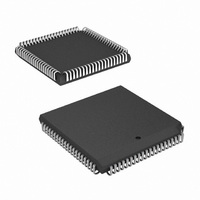
HSP45106JC-25Z Intersil, HSP45106JC-25Z Datasheet - Page 3

HSP45106JC-25Z
Manufacturer Part Number
HSP45106JC-25Z
Description
IC OSCILLATOR NCO 16BIT 84-PLCC
Manufacturer
Intersil
Type
Numerically Controlled Oscillator (NCO)r
Datasheet
1.HSP45106JC-25Z.pdf
(15 pages)
Specifications of HSP45106JC-25Z
Frequency
25.6MHz
Voltage - Supply
4.75 V ~ 5.25 V
Current - Supply
180mA
Operating Temperature
0°C ~ 70°C
Package / Case
84-PLCC
Lead Free Status / RoHS Status
Lead free / RoHS Compliant
Count
-
Available stocks
Company
Part Number
Manufacturer
Quantity
Price
Company:
Part Number:
HSP45106JC-25Z
Manufacturer:
Intersil
Quantity:
90
Pin Descriptions
DACSTRB
COS(15:0)
ENTIREG
MOD(2:0)
PAR/SER
SIN(15:0)
ENPHAC
Index Pin
INHOFR
INITPAC
INITTAC
BINFMT
PMSEL
NAME
TEST
TICO
PACI
OEC
OES
TYPE
O
O
O
O
I
I
I
I
I
I
I
I
I
I
I
I
I
(Continued)
Phase Accumulator Register Enable (active low). Registered on chip by CLK. When active, after being clocked onto
chip, ENPHAC enables the clocking of data into the Phase Accumulator Register.
Timer Increment Register Enable (active low). Registered on chip by CLK. When active, after being clocked onto
chip, ENTIREG enables the clocking of data into the Timer Increment Register.
Inhibit Offset Frequency Register Output (active low). Registered on chip by CLK. When active, after being clocked
onto chip, INHOFR zeroes the data path from the Offset Frequency Register to the Frequency Adder. New data
can be still clocked into the Offset Frequency Register. INHOFR does not affect the contents of the register.
Initialize Phase Accumulator (active low). Registered on chip by CLK. Zeroes the feedback path in the Phase
Accumulator. Does not clear the Phase Accumulator Register.
Modulation Control Inputs. When selected with the PMSEL line, these bits add an offset of 0, 45, 90, 135, 180,
225, 270, or 315 degrees to the current phase (i.e., modulate the output). The lower 13 bits of the phase control
are set to zero. These bits are registered when the Phase Offset Register is enabled.
Phase Modulation Select input. Registered on-chip by CLK. This input determines the source of the data clocked
into the Phase Offset Register. When high, the Phase Input Register is selected. When low, the external
modulation pins (MOD(2:1)) control the three most significant bits of the Phase Offset Register and the 13 least
significant bits are set to zero.
Phase Accumulator Carry Input (active low). Registered on-chip by CLK.
Initialize Timer Accumulator (active low). This input is registered on chip by CLK. When active, after being clocked
onto chip, INITTAC enables the clocking of data into the Timer increment Register, and also zeroes the feedback
path in the Timer Accumulator.
Test Select Input. Registered on chip by CLK. This input is active high. When active, this input enables test busses
to the outputs instead of the sine and cosine data.
Parallel/Serial Output Select. This input is registered on chip by CLK. When low, the sine and cosine outputs are
in serial mode. The Output Shift Registers will load in new data after ENPHAC goes low and will start shifting the
data out after ENPHAC goes high. When this input is high, the Output Registers are loaded every clock and no
shifting takes place.
Format. This input is registered on chip by CLK. When low, the MSB of the SIN and COS are inverted to form an
offset binary (unsigned) number.
Three-state control for bits SIN(15:0). Outputs are enabled when OES is low.
Three-state control for bits COS(15:0). Outputs are enabled when OEC is low.
Timer Accumulator Carry Output. Active low, registered. This output goes low when a carry is generated by the
Timer Accumulator.
DAC Strobe (active low). In serial mode, this output will go low when the first bit of a new output word is valid at
the shift register output. This pin is active only in serial mode.
Sine Output Data. When parallel mode is enabled, data is output on SIN(15:0). When serial mode is enabled,
output data bits are shifted out of SIN15 and SIN0. The bit stream on SIN15 is provided MSB first while the bit
stream on SIN0 is provided LSB first.
Cosine Output Data. When parallel mode is enabled, data is output on COS(15:0). When serial mode is enabled,
output data bits are shifted out of COS15 and COS0. The bit stream on COS15 is provided MSB first while the bit
stream in COS0 is provided LSB first.
Used to align chip in socket or on circuit board. Must be left as a no connect in circuit. (CPGA Package only).
3
HSP45106
DESCRIPTION
October 16, 2008
FN2809.8


