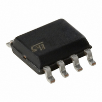
SA555D STMicroelectronics, SA555D Datasheet - Page 8

SA555D
Manufacturer Part Number
SA555D
Description
IC TIMER SGL BIPOLAR GP 8-SOIC
Manufacturer
STMicroelectronics
Type
555 Type, Timer/Oscillator (Single)r
Datasheet
1.NE555DT.pdf
(20 pages)
Specifications of SA555D
Frequency
500kHz
Voltage - Supply
4.5 V ~ 16 V
Current - Supply
10mA
Operating Temperature
-40°C ~ 105°C
Package / Case
8-SOIC (3.9mm Width)
Number Of Internal Timers
1
Supply Voltage (max)
16 V
Supply Voltage (min)
4.5 V
Maximum Operating Temperature
+ 105 C
Minimum Operating Temperature
- 40 C
Mounting Style
SMD/SMT
Lead Free Status / RoHS Status
Lead free / RoHS Compliant
Count
-
Lead Free Status / Rohs Status
Lead free / RoHS Compliant
Available stocks
Company
Part Number
Manufacturer
Quantity
Price
Part Number:
SA555D
Manufacturer:
S
Quantity:
20 000
Company:
Part Number:
SA555DR
Manufacturer:
Texas Instruments
Quantity:
20 000
Part Number:
SA555DR
Manufacturer:
TI/德州仪器
Quantity:
20 000
Company:
Part Number:
SA555DRG4
Manufacturer:
NEC
Quantity:
6 218
Company:
Part Number:
SA555DT
Manufacturer:
STMicroelectronics
Quantity:
68 143
Part Number:
SA555DT
Manufacturer:
ST
Quantity:
20 000
Application information
4
4.1
8/20
Application information
Monostable operation
In the monostable mode, the timer generates a single pulse. As shown in
external capacitor is initially held discharged by a transistor inside the timer.
Figure 12. Typical schematics in monostable operation
The circuit triggers on a negative-going input signal when the level reaches 1/3 V
triggered, the circuit remains in this state until the set time has elapsed, even if it is triggered
again during this interval. The duration of the output HIGH state is given by t = 1.1 R
is easily determined by
Note that because the charge rate and the threshold level of the comparator are both
directly proportional to supply voltage, the timing interval is independent of supply. Applying
a negative pulse simultaneously to the reset terminal (pin 4) and the trigger terminal (pin 2)
during the timing cycle discharges the external capacitor and causes the cycle to start over.
The timing cycle now starts on the positive edge of the reset pulse. During the time the reset
pulse is applied, the output is driven to its LOW state.
When a negative trigger pulse is applied to pin 2, the flip-flop is set, releasing the short-
circuit across the external capacitor and driving the output HIGH. The voltage across the
capacitor increases exponentially with the time constant t = R
the capacitor equals 2/3 V
capacitor rapidly and drives the output to its LOW state.
Figure 13
When Reset is not used, it should be tied high to avoid any possibility of unwanted
triggering.
shows the actual waveforms generated in this mode of operation.
Trigger
Output
V
CC
= 5 to 15V
Figure
CC
, the comparator resets the flip-flop which then discharges the
14.
2
3
Reset
4
NE555
1
8
7
5
6
1
Control Voltage
C
1
. When the voltage across
NE555 - SA555 - SE555
0.01
R1
μ
C1
Figure
F
12, the
CC
1
. Once
C
1
and


