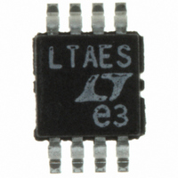
LTC6904CMS8#PBF Linear Technology, LTC6904CMS8#PBF Datasheet - Page 9

LTC6904CMS8#PBF
Manufacturer Part Number
LTC6904CMS8#PBF
Description
IC OSC PROGRAM I2C INTRFC 8-MSOP
Manufacturer
Linear Technology
Type
Oscillator, Siliconr
Datasheet
1.LTC6903CMS8.pdf
(12 pages)
Specifications of LTC6904CMS8#PBF
Frequency
68MHz
Voltage - Supply
2.7 V ~ 5.5 V
Current - Supply
7mA
Operating Temperature
-40°C ~ 85°C
Package / Case
8-MSOP, Micro8™, 8-uMAX, 8-uSOP,
Leaded Process Compatible
Yes
Rohs Compliant
Yes
Peak Reflow Compatible (260 C)
Yes
Supply Voltage Range
2.7V To 5.5V
Digital Ic Case Style
MSOP
No. Of Pins
8
Operating Temperature Range
-40°C To +85°C
Lead Free Status / RoHS Status
Lead free / RoHS Compliant
Count
-
Available stocks
Company
Part Number
Manufacturer
Quantity
Price
Serial Port Register Description
OCT[3:0] – Frequency Divider Setting. (See Frequency
Setting Section)
DAC[9:0] – Master Oscillator Frequency Setting. (See
Frequency Setting Section)
CNF[1:0] – Output Configuration. This controls outputs
CLK and CLK according to Table 2.
LTC6903 SPI Compatible Interface
A serial data transfer is composed of sixteen (16) bits of
data labeled D15 through D0. D15 is the first bit of data
presented in each transaction. All serial port register bits
are set LOW on power-up.
applicaTions inFormaTion
Timing Diagrams
SDA
SCL
START
0
0
1
0
0
2
SDA
SCL
t
HD, STA
1
1
3
CONDITION
Typical LTC6904 Input Waveform—Programming Frequency to 68MHz (ADR Pin Set LOW)
ADDRESS
START
0
0
4
1
1
5
t
LOW
1
6
1
ADR
t
r
1
7
t
HIGH
t
SU, DAT
WR
0
8
t
f
ACK
9
OCT3 OCT2 OCT1 OCT0 DAC9 DAC8 DAC7 DAC6
1
1
t
HD, DAT
Timing Diagram (LTC6904)
1
2
1
3
1
4
REPEATED START
CONDITION
1
5
Writing Data (LTC6903 Only)
When the SEN line is brought LOW, serial data presented
on the SDI input is clocked in on the rising edges of SCK
until SEN is brought HIGH. On every eighth rising edge
of SCK, the preceding 8-bits of data are clocked into the
internal register. It is therefore possible to clock in only
the 8 {D15 - D8} most significant bits of data rather than
completing an entire transfer.
The serial data transfer starts with the most significant
bit and ends with the least significant bit of the data, as
shown in the timing diagram.
1
6
t
SU, STA
1
7
t
HD, STA
1
8
ACK
9
DAC5 DAC4 DAC3 DAC2 DAC1 DAC0 CNF1 CNF0
1
1
LTC6903/LTC6904
1
2
CONDITION
1
3
STOP
1
4
t
SU, STO
t
BUF
1
5
CONDITION
START
1
6
6903 TD02
0
7
0
8
ACK
9
STOP
69034fc
6903 TD03


