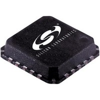
SI5310-BM Silicon Laboratories Inc, SI5310-BM Datasheet - Page 6

SI5310-BM
Manufacturer Part Number
SI5310-BM
Description
IC CLOCK MULTIPLIER/REGEN 20MLP
Manufacturer
Silicon Laboratories Inc
Type
Clock Multiplierr
Datasheet
1.SI5310-BM.pdf
(26 pages)
Specifications of SI5310-BM
Package / Case
20-VQFN Exposed Pad, 20-HVQFN, 20-SQFN, 20-DHVQFN
Pll
Yes with Bypass
Input
Clock
Output
CML
Number Of Circuits
1
Ratio - Input:output
1:2
Differential - Input:output
Yes/Yes
Frequency - Max
668MHz
Divider/multiplier
Yes/Yes
Voltage - Supply
2.375 V ~ 2.625 V
Operating Temperature
-40°C ~ 85°C
Mounting Type
Surface Mount
Frequency-max
668MHz
Mounting Style
SMD/SMT
Description/function
Multiplier/Regenratr 155MHz 622MHz
Lead Free Status / RoHS Status
Contains lead / RoHS non-compliant
Other names
336-1139
Table 2. DC Characteristics, V
(V
Si5310
6
Parameter
Supply Current
MULTSEL = 0
MULTSEL = 1
Power Dissipation
MULTSEL = 0
MULTSEL = 1
Common Mode Input Voltage
(CLKIN, REFCLK)
Input Voltage Range*
(CLKIN+, CLKIN–, REFCLK+, REFCLK–)
Differential Input Voltage Swing*
(CLKIN, REFCLK)
Input Impedance (CLKIN, REFCLK)
Differential Output Voltage Swing
(CLKOUT)
Differential Output Voltage Swing
(MULTOUT)
Output Common Mode Voltage
(CLKOUT, MULTOUT)
Output Impedance (CLKOUT, MULTOUT)
Output Short to GND (CLKOUT, MULTOUT)
Output Short to V
Input Voltage Low (LVTTL Inputs)
Input Voltage High (LVTTL Inputs)
Input Low Current (LVTTL Inputs)
Input High Current (LVTTL Inputs)
Output Voltage Low (LVTTL Outputs)
Output Voltage High (LVTTL Outputs)
Input Impedance (LVTTL Inputs)
PWRDN/CAL Internal Pulldown Current
*Note: The CLKIN and REFCLK inputs may be driven differentially or single-endedly. When driving single-endedly, the voltage
DD
= 2.5 V ±5%, T
swing of the signal applied to the active input must exceed the specified minimum Differential Input Voltage Swing (V
min) and the unused input must be ac-coupled to ground. When driving differentially, the difference between the
positive and negative input signals must exceed V
range.) In either case, the voltage applied to any individual pin (CLKIN+, CLKIN–, REFCLK+, or REFCLK–) must not
exceed the specified maximum Input Voltage Range (V
DD
A
= –40 to 85 °C)
(CLKOUT, MULTOUT)
DD
= 2.5 V, 622 Mbps (MULTSEL = 0)
Symbol
I
PWRDN
V
R
I
I
V
V
V
V
SC(–)
SC(+)
V
R
R
I
V
V
V
V
P
OCM
I
DD
OUT
I
ICM
OD
OD
IH
OH
IL
OL
ID
IH
IS
IN
IN
D
IL
ID
Rev. 1.2
min. (Each individual input signal needs to swing only half of this
IS
V
Test Condition
Single-ended
See Figure 1
See Figure 1
See Figure 1
PWRDN
max).
Line-to-Line
100 Ω Load
Line-to-Line
100 Ω Load
Line-to-Line
100 Ω Load
Line-to-Line
I
I
O
O
= 2 mA
= 2 mA
≥ 0.8 V
–17.5
Min
780
780
200
200
2.0
2.0
84
84
10
15
—
—
—
—
—
—
—
—
—
—
—
.80 x V
V
–14.5
Typ
124
293
310
100
970
970
0.23
100
117
DD
25
25
—
—
—
—
—
—
—
—
—
–
DD
1500
1260
1260
Max
127
134
333
352
750
116
116
0.4
31
10
10
45
—
—
—
—
—
—
.8
mV
mV
mV
Unit
mW
mA
mV
mA
mA
µA
µA
kΩ
µA
Ω
Ω
V
V
V
V
V
V
PP
PP
PP
ID


