LMX2353SLBX National Semiconductor, LMX2353SLBX Datasheet - Page 9
LMX2353SLBX
Manufacturer Part Number
LMX2353SLBX
Description
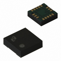
IC FREQ SYNTH 2.5GHZ 16LAMCSP
Manufacturer
National Semiconductor
Series
PLLatinum™r
Type
PLL Frequency Synthesizerr
Datasheet
1.LMX2353TMNOPB.pdf
(19 pages)
Specifications of LMX2353SLBX
Pll
Yes with Bypass
Input
CMOS, TTL
Output
CMOS
Number Of Circuits
1
Ratio - Input:output
2:1
Differential - Input:output
Yes/No
Frequency - Max
2.5GHz
Divider/multiplier
Yes/Yes
Voltage - Supply
2.7 V ~ 5.5 V
Operating Temperature
-40°C ~ 85°C
Mounting Type
Surface Mount
Package / Case
16-Laminate CSP
Frequency-max
2.5GHz
Lead Free Status / RoHS Status
Lead free / RoHS Compliant
Other names
LMX2353SLBX/NOPB
LMX2353SLBXTR
LMX2353SLBXTR
Available stocks
Company
Part Number
Manufacturer
Quantity
Price
Company:

Part Number:
LMX2353SLBX
Manufacturer:
ON
Quantity:
100


1.0 Functional Description
1.8 F
The F
programming description 2.4.2 for more details.
1.8.1 Lock Detect Output
A digital filtered lock detect function is included with each phase detector through an internal digital filter to produce a logic level
output available on the F
inputs is less than 15 ns for 5 consecutive comparison cycles. The lock detect output is low when the error between the phase
detector inputs is more than 30 ns for one comparison cycle. An analog lock detect status generated from the phase detector is
also available on the F
when the charge pump is active during a comparison cycle. When a PLL is in power down mode, the respective lock detect output
is always low. See programming descriptions 2.4.2.2 - 2.4.2.4.
1.9 OUT0/OUT1 Output Modes (FastLock & CMOS Output Modes)
The OUT_0 and OUT_1 pins are normally used as general purpose CMOS outputs or as part of a FastLock scheme. There is also
a production test mode that overrides the other two normal modes when activated. The selection of these modes is determined
by the 4 bit CMOS register (F2_15–18) described in Table 2.5.3.
The FastLock mode allows the user to open up the loop bandwidth momentarily while acquiring lock by increasing the charge
pump output current magnitude while simultaneously switching in a second resistor element to ground via the OUT0 output pin.
The loop will lock faster without any additional stability considerations as the phase margin remains constant.
The loop bandwidth during FastLock can be opened up by as much as a factor of 4. The amount of bandwidth increase is a
function of the square root of the charge pump current increase. The maximum charge pump current ratio results from switching
the charge pump current between 100 µA and 1.6 mA. The damping resistor ratio for these two charge pump current setting
changes by the reciprocal of the bandwidth change. In the 4 to 1 bandwidth scenerio, the resulting damping resistor value would
be 1/4th of the steady state value. This would be achieved by switching 3 more identical resistors in parallel with the first to ground
through the OUT_0 pin.
1.10 POWER CONTROL
The PLL is power controlled by the device enable pin (CE) or MICROWIRE power down bit. The enable pin overrides the power
down bit except for the V2_EN bit. When CE is high, the power down bit determines the state of power control. Activation of any
PLL power down mode results in the disabling of the N counter and de-biasing of f
counter functionality also becomes disabled when the power down bit is activated. The reference oscillator block powers down
and the OSC
is high . Power down forces the charge pump and phase comparator logic to a TRISTATE condition. A power down counter reset
function resets both N and R counters. Upon powering up the N counter resumes counting in “close” alignment with the R counter
(The maximum error is one prescaler cycle). The MICROWIRE control register remains active and capable of loading and latching
in data during all of the power down modes.
2.0 Programming Description
2.1 MICROWIRE INTERFACE
The LMX2353 register set can be accessed through the
MICROWIRE interface. A 24-bit shift register is used as a
temporary register to indirectly program the on-chip regis-
ters. The shift register consists of a 24-bit DATA[21:0] field
and a 2-bit ADDRESS[1:0] field as shown below. The ad-
dress field is used to decode the internal register address.
Data is clocked into the shift register in the direction from
MSB to LSB, when the CLK signal goes high. On the rising
edge of Latch Enable (LE) signal, data stored in the shift
register is loaded into the addressed latch.
2.1.1 Registers’ Address Map
When Latch Enable (LE) is transitioned high, data is trans-
ferred from the 24-bit shift register into the appropriate latch
depending on the state of the ADDRESS[1:0] bits. A multi-
plexing circuit decodes these address bits and writes the
data field to the corresponding internal register.
MSB
23
O
o
LD Multifunction Output
LD output pin can deliver several internal functions including analog/digital lock detects, and counter outputs. See
DATA [21:0]
IN
pin reverts to a high impedance state when CE or power down bit’s are asserted, unless the V2_EN bit (R[20])
O
LD output pin, if selected. The lock detect output goes high when the charge pump is inactive. It goes low
O
LD output pin if selected. The lock detect output is high when the error between the phase detector
2
1
ADDRESS [1:0]
(Continued)
LSB
0
9
ADDRESS[1:0]
0
0
1
1
FIELD
IN
input (to a high impedance state). The R
0
1
0
1
F1 Register
F2 Register
R Register
N Register
ADDRESSED
REGISTER
www.national.com
Related parts for LMX2353SLBX
Image
Part Number
Description
Manufacturer
Datasheet
Request
R

Part Number:
Description:
Pllatinum? Fractional N Single 2.5 Ghz Low Power Frequency Synthesizer
Manufacturer:
National Semiconductor Corporation
Datasheet:

Part Number:
Description:
National Semiconductor [8-Bit D/A Converter]
Manufacturer:
National Semiconductor
Datasheet:
Part Number:
Description:
National Semiconductor [Media Coprocessor]
Manufacturer:
National Semiconductor
Datasheet:
Part Number:
Description:
Digitally Controlled Tone and Volume Circuit with Stereo Audio Power Amplifier, Microphone Preamp Stage and National 3D Sound
Manufacturer:
National Semiconductor
Datasheet:
Part Number:
Description:
Digitally Controlled Tone and Volume Circuit with Stereo Audio Power Amplifier, Microphone Preamp Stage and National 3D Sound
Manufacturer:
National Semiconductor
Datasheet:
Part Number:
Description:
AC97 Rev 2 Codec with Sample Rate Conversion and National 3D Sound
Manufacturer:
National Semiconductor
Part Number:
Description:
Manufacturer:
National Semiconductor
Datasheet:
Part Number:
Description:
Manufacturer:
National Semiconductor
Datasheet:
Part Number:
Description:
General Purpose, Low Voltage, Low Power, Rail-to-Rail Output Operational Amplifiers
Manufacturer:
National Semiconductor
Datasheet:
Part Number:
Description:
8-bit 20 MSPS flash A/D converter.
Manufacturer:
National Semiconductor
Datasheet:
Part Number:
Description:
Low Noise Quad Operational Amplifier
Manufacturer:
National Semiconductor
Datasheet:
Part Number:
Description:
Quad Differential Line Receivers
Manufacturer:
National Semiconductor
Datasheet:
Part Number:
Description:
Quad High Speed Trapezoidal? Bus Transceiver
Manufacturer:
National Semiconductor
Datasheet:
Part Number:
Description:
Dual Line Receiver
Manufacturer:
National Semiconductor
Datasheet: