CY28442ZXC-2 Cypress Semiconductor Corp, CY28442ZXC-2 Datasheet - Page 2
CY28442ZXC-2
Manufacturer Part Number
CY28442ZXC-2
Description
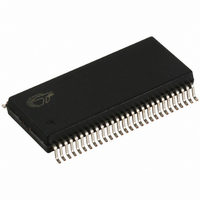
IC CLOCK GEN ALVISO 56-TSSOP
Manufacturer
Cypress Semiconductor Corp
Type
Fanout Distribution, Spread Spectrum Clock Generatorr
Datasheet
1.CY28442ZXC-2.pdf
(21 pages)
Specifications of CY28442ZXC-2
Pll
Yes with Bypass
Input
LVTTL, Crystal
Output
Clock
Number Of Circuits
1
Ratio - Input:output
11:15
Differential - Input:output
No/Yes
Frequency - Max
200MHz
Divider/multiplier
Yes/No
Voltage - Supply
3.135 V ~ 3.465 V
Operating Temperature
0°C ~ 85°C
Mounting Type
Surface Mount
Package / Case
56-TSSOP II
Frequency-max
100MHz
Lead Free Status / RoHS Status
Lead free / RoHS Compliant
Available stocks
Company
Part Number
Manufacturer
Quantity
Price

Part Number:
CY28442ZXC-2
Manufacturer:
CYP
Quantity:
20 000
Company:
Part Number:
CY28442ZXC-2T
Manufacturer:
TI
Quantity:
11


Document #: 38-07691 Rev. *B
Pin Definitions
1
2
33,32
7
6
3,4,5
8
9
10
11
12
13
14,15
16
17,18
19,20,22,23,
24,25,30,31
21,28
34
26,27
29
36,35
37
38
39
42
44,43,41,40
45
46
47
Pin No.
VDD_48
VSS_48
DOT96T, DOT96C
96_100_SSC
VDD_SRC
SRC4_SATAT,
CPUT2_ITP/SRCT7,
VDDA
SCLK
VDD_REF
VSS_REF
CLKREQA#/SRCT6,
CLKREQB#,SRCC6
VDD_PCI
VSS_PCI
PCI
ITP_EN/PCIF0
PCIF1/96_100_SEL
VTT_PWRGD#/PD
FS_A/48_M0
FS_B/TEST_MODE
SRCT/C
VDD_SRC_ITP
SRC4_SATAC
VSS_SRC
CPUC2_ITP/SRCC7
VSSA
IREF
VDD_CPU
CPUT/C
VSS_CPU
SDATA
Name
I/O, PU 3.3V LVTTL input for enabling assigned SRC clock (active LOW) or 100-MHz
I/O, SE 3.3V LVTTL input to enable SRC7 or CPU2_ITP/33-MHz clock output.
PD,SE
O, DIF Fixed 96-MHz clock output.
O, DIF 100-MHz Differential serial reference clocks.
O, DIF Differential serial reference clock. Recommended output for SATA.
O, DIF Selectable differential CPU or SRC clock output.
O, DIF Differential CPU clock outputs.
O, SE 33-MHz clock
O,DIF Differential 96-/100-MHz SS clock for flat-panel display
PWR 3.3V power supply for output
PWR 3.3V power supply for outputs.
PWR 3.3V power supply for outputs.
PWR 3.3V power supply for outputs.
PWR 3.3V power supply for outputs.
PWR 3.3V power supply for PLL.
PWR 3.3V power supply for outputs.
GND
GND
I, PU
GND
GND
GND
GND
Type
I/O,
I/O
I/O
I
I
I
Ground for outputs.
Serial Reference Clock.
Selectable through CLKREQA# defaults to enable/disable SRCT/C4, CLKREQB#
defaults to enable/disable SRCT/C5. Assignment can be changed via SMBUS
register Byte 8.
Ground for outputs.
(sampled on the VTT_PWRGD# assertion).
1 = CPU2_ITP, 0 = SRC7
33-MHz clock/3.3V-tolerant input for 96_100M frequency selection
(sampled on the VTT_PWRGD# assertion).
1 = 100 MHz, 0 = 96 MHz
3.3V LVTTL input. This pin is a level sensitive strobe used to latch the FS_A,
FS_B, FS_C and ITP_EN, 96MSS_SRC_SEL inputs, SEL_CLKREQ. After
VTT_PWRGD# (active LOW) assertion, this pin becomes a real-time input for
asserting power-down (active HIGH).
3.3V-tolerant input for CPU frequency selection/fixed 48-MHz clock output.
Refer to DC Electrical Specifications table for Vil_FS and Vih_FS specifications.
Ground for outputs.
3.3V-tolerant input for CPU frequency selection. Selects Ref/N or Tri-state
when in test mode
0 = Tri-state, 1 = Ref/N
Refer to DC Electrical Specifications table for Vil_FS and Vih_FS specifications.
Ground for outputs.
ITP_EN = 0 @ VTT_PWRGD# assertion = SRC7
ITP_EN = 1 @ VTT_PWRGD# assertion = CPU2
Ground for PLL.
A precision resistor is attached to this pin, which is connected to the internal
current reference.
Ground for outputs.
SMBus-compatible SCLOCK.
SMBus-compatible SDATA.
Description
CY28442-2
Page 2 of 21
Related parts for CY28442ZXC-2
Image
Part Number
Description
Manufacturer
Datasheet
Request
R

Part Number:
Description:
Manufacturer:
Cypress Semiconductor Corp
Datasheet:
Part Number:
Description:
Manufacturer:
Cypress Semiconductor Corp
Datasheet:
Part Number:
Description:
Manufacturer:
Cypress Semiconductor Corp
Datasheet:
Part Number:
Description:
Manufacturer:
Cypress Semiconductor Corp
Datasheet:
Part Number:
Description:
Manufacturer:
Cypress Semiconductor Corp
Datasheet: