CY28442ZXC Cypress Semiconductor Corp, CY28442ZXC Datasheet - Page 12
CY28442ZXC
Manufacturer Part Number
CY28442ZXC
Description
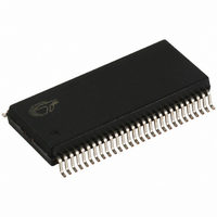
IC CLOCK GEN ALVISO 56-TSSOP
Manufacturer
Cypress Semiconductor Corp
Type
Fanout Distribution, Spread Spectrum Clock Generatorr
Datasheet
1.CY28442ZXC.pdf
(22 pages)
Specifications of CY28442ZXC
Pll
Yes with Bypass
Input
LVTTL, Crystal
Output
Clock
Number Of Circuits
1
Ratio - Input:output
11:15
Differential - Input:output
No/Yes
Frequency - Max
200MHz
Divider/multiplier
Yes/No
Voltage - Supply
3.135 V ~ 3.465 V
Operating Temperature
0°C ~ 85°C
Mounting Type
Surface Mount
Package / Case
56-TSSOP II
Frequency-max
100MHz
Lead Free Status / RoHS Status
Lead free / RoHS Compliant
Available stocks
Company
Part Number
Manufacturer
Quantity
Price

Part Number:
CY28442ZXC-2
Manufacturer:
CYP
Quantity:
20 000
Company:
Part Number:
CY28442ZXC-2T
Manufacturer:
TI
Quantity:
11
Company:
Part Number:
CY28442ZXC-4
Manufacturer:
SEMTEC
Quantity:
946


Document #: 38-07680 Rev. **
PD Deassertion
The power-up latency is less than 1.8 ms. This is the time from
the deassertion of the PD pin or the ramping of the power
supply until the time that stable clocks are output from the
clock chip. All differential outputs stopped in a three-state
CPU_STP# Assertion
The CPU_STP# signal is an active low input used for
synchronous stopping and starting the CPU output clocks
while the rest of the clock generator continues to function.
When the CPU_STP# pin is asserted, all CPU outputs that are
set with the SMBus configuration to be stoppable via assertion
of CPU_STP# will be stopped within two–six CPU clock
CPUC, 133MHz
CPUT, 133MHz
SRCC 100MHz
SRCT 100MHz
PCI, 33 MHz
USB, 48MHz
DOT96C
DOT96T
CPUC, 133MHz
CPUT, 133MHz
SRCC 100MHz
SRCT 100MHz
USB, 48MHz
PCI, 33MHz
REF
PD
DOT96C
DOT96T
REF
Figure 5. Power-down Deassertion Timing Waveform
PD
Figure 4. Power-down Assertion Timing Waveform
ADVANCE INFORMATION
<300µS, >200mV
Tdrive_PWRDN#
Tstable
<1.8nS
condition resulting from power down will be driven high in less
than 300 µs of PD deassertion to a voltage greater than 200
mV. After the clock chip’s internal PLL is powered up and
locked, all outputs will be enabled within a few clock cycles of
each other. Below is an example showing the relationship of
clocks coming up.
periods after being sampled by two rising edges of the internal
CPUC clock. The final states of the stopped CPU signals are
CPUT = HIGH and CPUC = LOW. There is no change to the
output drive current values during the stopped state. The
CPUT is driven HIGH with a current value equal to 6 x (Iref),
and the CPUC signal will be Tri-stated.
CY28442
Page 12 of 22
[+] Feedback
Related parts for CY28442ZXC
Image
Part Number
Description
Manufacturer
Datasheet
Request
R

Part Number:
Description:
Manufacturer:
Cypress Semiconductor Corp
Datasheet:
Part Number:
Description:
Manufacturer:
Cypress Semiconductor Corp
Datasheet:
Part Number:
Description:
Manufacturer:
Cypress Semiconductor Corp
Datasheet:
Part Number:
Description:
Manufacturer:
Cypress Semiconductor Corp
Datasheet:
Part Number:
Description:
Manufacturer:
Cypress Semiconductor Corp
Datasheet: