CY28411ZXC Cypress Semiconductor Corp, CY28411ZXC Datasheet - Page 4
CY28411ZXC
Manufacturer Part Number
CY28411ZXC
Description
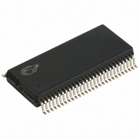
IC CLOCK GEN ALVISO 56TSSOP
Manufacturer
Cypress Semiconductor Corp
Type
Fanout Distribution, Spread Spectrum Clock Generatorr
Datasheet
1.CY28411ZXC.pdf
(19 pages)
Specifications of CY28411ZXC
Pll
Yes
Input
LVTTL, Crystal
Output
Clock
Number Of Circuits
1
Ratio - Input:output
7:20
Differential - Input:output
No/Yes
Frequency - Max
266MHz
Divider/multiplier
Yes/No
Voltage - Supply
3.135 V ~ 3.465 V
Operating Temperature
0°C ~ 85°C
Mounting Type
Surface Mount
Package / Case
56-TSSOP II
Frequency-max
100MHz
Lead Free Status / RoHS Status
Lead free / RoHS Compliant
Available stocks
Company
Part Number
Manufacturer
Quantity
Price

Company:
Part Number:
CY28411ZXC-1
Manufacturer:
CY
Quantity:
42
Company:
Part Number:
CY28411ZXC-1
Manufacturer:
CY
Quantity:
880


Document #: 38-07594 Rev. *B
Table 3. Block Read and Block Write Protocol (continued)
Table 4. Byte Read and Byte Write Protocol
Control Registers
Byte 0:Control Register 0
36:29
45:38
18:11
27:20
Bit
8:2
Bit
Bit
28
37
46
....
....
....
....
10
19
28
29
1
9
7
6
5
4
3
Acknowledge from slave
Data byte 1 – 8 bits
Acknowledge from slave
Data byte 2 – 8 bits
Acknowledge from slave
Data Byte /Slave Acknowledges
Data Byte N –8 bits
Acknowledge from slave
Stop
Start
Slave address – 7 bits
Write
Acknowledge from slave
Command Code – 8 bits
Acknowledge from slave
Data byte – 8 bits
Acknowledge from slave
Stop
@Pup
1
1
1
1
1
Block Write Protocol
Byte Write Protocol
CPUC2_ITP/SRCC7
CPUT2_ITP/SRCT7
Description
Description
SRC[T/C]6
SRC[T/C]5
SRC[T/C]4
SRC[T/C]3
Name
CPU[T/C]2_ITP/SRC[T/C]7 Output Enable
0 = Disable (Hi-Z), 1 = Enable
SRC[T/C]6 Output Enable
0 = Disable (Hi-Z), 1 = Enable
SRC[T/C]5 Output Enable
0 = Disable (Hi-Z), 1 = Enable
SRC[T/C]4 Output Enable
0 = Disable (Hi-Z), 1 = Enable
SRC[T/C]3 Output Enable
0 = Disable (Hi-Z), 1 = Enable
27:21
37:30
46:39
55:48
27:21
37:30
18:11
Bit
28
29
38
47
56
....
....
....
....
8:2
Bit
10
19
20
28
29
38
39
1
9
Data byte 1 from slave – 8 bits
Slave address – 7 bits
Read = 1
Acknowledge from slave
Byte Count from slave – 8 bits
Acknowledge
Acknowledge
Data byte 2 from slave – 8 bits
Acknowledge
Data bytes from slave / Acknowledge
Data Byte N from slave – 8 bits
NOT Acknowledge
Stop
Start
Slave address – 7 bits
Write
Acknowledge from slave
Command Code – 8 bits
Acknowledge from slave
Repeated start
Slave address – 7 bits
Read
Acknowledge from slave
Data from slave – 8 bits
NOT Acknowledge
Stop
Description
Block Read Protocol
Byte Read Protocol
Description
Description
CY28411
Page 4 of 19
[+] Feedback
Related parts for CY28411ZXC
Image
Part Number
Description
Manufacturer
Datasheet
Request
R

Part Number:
Description:
Manufacturer:
Cypress Semiconductor Corp
Datasheet:
Part Number:
Description:
Manufacturer:
Cypress Semiconductor Corp
Datasheet:
Part Number:
Description:
Manufacturer:
Cypress Semiconductor Corp
Datasheet:
Part Number:
Description:
Manufacturer:
Cypress Semiconductor Corp
Datasheet:
Part Number:
Description:
Manufacturer:
Cypress Semiconductor Corp
Datasheet: