CY28411ZXC Cypress Semiconductor Corp, CY28411ZXC Datasheet
CY28411ZXC
Specifications of CY28411ZXC
Available stocks


Related parts for CY28411ZXC

CY28411ZXC Summary of contents
Page 1
... IREF PD PLL2 2 SDATA I C Logic SCLK Cypress Semiconductor Corporation Document #: 38-07594 Rev. *B Clock Generator for Intel • 33-MHz PCI clock • Low-voltage frequency select input 2 • support with readback capabilities • Ideal Lexmark Spread Spectrum profile for maximum electromagnetic interference (EMI) reduction • ...
Page 2
Pin Definitions Pin No. Name 54 CPU_STP# 44,43,41,40 CPUT/C O, DIF Differential CPU clock outputs. 36,35 CPUT2_ITP/SRCT7, O, DIF Selectable differential CPU or SRC clock output. CPUC2_ITP/SRCC7 14,15 DOT96T, DOT96C O, DIF Fixed 96-MHz clock output. 12 FS_A/USB_48 I/O, SE ...
Page 3
Frequency Select Pins (FS_A, FS_B and FS_C) Host clock frequency selection is achieved by applying the appropriate logic levels to FS_A, FS_B, FS_C inputs prior to VTT_PWRGD# assertion (as seen by the clock synthesizer). Upon VTT_PWRGD# being sampled low by ...
Page 4
Table 3. Block Read and Block Write Protocol (continued) Block Write Protocol Bit Description 28 Acknowledge from slave 36:29 Data byte 1 – 8 bits 37 Acknowledge from slave 45:38 Data byte 2 – 8 bits 46 Acknowledge from slave ...
Page 5
Byte 0:Control Register 0 (continued) Bit @Pup Name 2 1 SRC[T/C SRC[T/C SRC[T/C]0 Byte 1: Control Register 1 Bit @Pup Name 7 1 PCIF0 6 1 DOT_96T USB_48 4 1 REF 3 0 Reserved ...
Page 6
Byte 3: Control Register 3 (continued) Bit @Pup Name 4 0 SRC4 3 0 SRC3 2 0 SRC2 1 0 SRC1 0 0 SRC0 Byte 4: Control Register 4 Bit @Pup Name 7 0 Reserved 6 0 DOT96T ...
Page 7
Byte 6: Control Register 6 Bit @Pup Name Reserved 4 1 REF 3 1 PCIF, SRC, PCI 2 Externally CPUT/C selected 1 Externally CPUT/C selected 0 Externally CPUT/C selected Byte 7: Vendor ID Bit ...
Page 8
Calculating Load Capacitors In addition to the standard external trim capacitors, trace capacitance and pin capacitance must also be considered to correctly calculate crystal loading. As mentioned previously, the capacitance on each side of the crystal is in series with ...
Page 9
PD (Power-down) Clarification The VTT_PWRGD# /PD pin is a dual function pin. During initial power-up, the pin functions as VTT_PWRGD#. Once VTT_PWRGD# has been sampled low by the clock chip, the pin assumes PD functionality. The PD pin is an ...
Page 10
CPU_STP# Assertion The CPU_STP# signal is an active low input used for synchronous stopping and starting the CPU output clocks while the rest of the clock generator continues to function. When the CPU_STP# pin is asserted, all CPU outputs that ...
Page 11
CPU_STOP# PD CPUT(Free Running) CPUC(Free Running) CPUT(Stoppable) CPUC(Stoppable) DOT96T DOT96C Figure 8. CPU_STP# = Hi-Z, CPU_PD = Hi-Z, DOT_PD = tHi-Z [1] PCI_STP# Assertion The PCI_STP# signal is an active LOW input used for synchronous stopping and starting the PCI ...
Page 12
FS_A, FS_B,FS_C VTT_PW RGD# PW RGD_VRM 0.2-0.3mS VDD Clock Gen Clock State State 0 Off Clock Outputs Off Clock VCO VDD_A = 2.0V S0 Power Off Figure 12. Clock Generator Power-up/Run State Diagram Document #: 38-07594 Rev ait ...
Page 13
Absolute Maximum Conditions Parameter Description V Core Supply Voltage DD V Analog Supply Voltage DD_A V Input Voltage IN T Temperature, Storage S T Temperature, Operating Ambient A T Temperature, Junction J Ø Dissipation, Junction to Case JC (Mil-Spec 883E ...
Page 14
AC Electrical Specifications Parameter Description Crystal T XIN Duty Cycle DC T XIN Period PERIOD XIN Rise and Fall Times XIN Cycle to Cycle Jitter CCJ L Long-term Accuracy ACC CPU at 0.7V T ...
Page 15
AC Electrical Specifications (continued) Parameter Description T SRCT/C Cycle to Cycle Jitter CCJ L SRCT/C Long Term Accuracy ACC SRCT and SRCC Rise and Fall Times Rise/Fall Matching RFM ∆T Rise TimeVariation R ∆T ...
Page 16
AC Electrical Specifications (continued) Parameter Description T Period PERIOD T Absolute Period PERIODAbs T USB high time HIGH T USB low time LOW Rise and Fall Times Cycle to Cycle Jitter CCJ REF T ...
Page 17
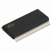
... SSOP – Tape and Reel CY28411ZC 56-pin TSSOP CY28411ZCT 56-pin TSSOP – Tape and Reel Lead-free (Planned) CY28411OXC 56-pin SSOP CY28411OXCT 56-pin SSOP – Tape and Reel CY28411ZXC 56-pin TSSOP CY28411ZXCT 56-pin TSSOP – Tape and Reel Document #: 38-07594 Rev Ω D iff tia Ω ...
Page 18
Package Diagrams 56-Lead Shrunk Small Outline Package O56 28 29 0.720 0.730 0.088 0.092 0.025 BSC 56-Lead Thin Shrunk Small Outline Package, Type mm) Z56 0.249[0.009 13.894[0.547] 14.097[0.555] 0.851[0.033] 0.500[0.020] 0.950[0.037] BSC 2 ...
Page 19
Document History Page Document Title: CY28411 Clock Generator for Intel Document Number: 38-07594 REV. ECN NO. Issue Date ** 130205 12/24/03 *A 207715 See ECN *B 229428 See ECN Document #: 38-07594 Rev. *B Alviso Chipset Orig. of Change ...