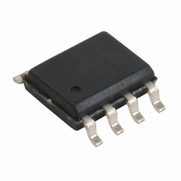
W181-01G Cypress Semiconductor Corp, W181-01G Datasheet - Page 5

W181-01G
Manufacturer Part Number
W181-01G
Description
CLOCK EMI REDUCTION SSCG 8-SOIC
Manufacturer
Cypress Semiconductor Corp
Series
Premis™r
Type
Clock/Frequency Synthesizer, Spread Spectrum Clock Generatorr
Datasheet
1.W181-01G.pdf
(9 pages)
Specifications of W181-01G
Pll
Yes
Input
Clock, Crystal
Output
CMOS
Number Of Circuits
1
Ratio - Input:output
1:1
Differential - Input:output
No/No
Frequency - Max
75MHz
Divider/multiplier
Yes/No
Voltage - Supply
3.135 V ~ 5.5 V
Operating Temperature
0°C ~ 70°C
Mounting Type
Surface Mount
Package / Case
8-SOIC (3.9mm Width)
Frequency-max
75MHz
Lead Free Status / RoHS Status
Contains lead / RoHS non-compliant
Other names
428-1395
Available stocks
Company
Part Number
Manufacturer
Quantity
Price
Company:
Part Number:
W181-01G
Manufacturer:
TEXAS
Quantity:
224
Part Number:
W181-01G
Manufacturer:
CYPRESS/赛普拉斯
Quantity:
20 000
Part Number:
W181-01GI
Manufacturer:
CYPRESS/赛普拉斯
Quantity:
20 000
Part Number:
W181-01GT
Manufacturer:
PTC
Quantity:
20 000
Document #: 38-07152 Rev. *D
.
Absolute Maximum Conditions
DC Electrical Characteristics
DC Electrical Characteristics:
V
T
T
T
P
I
t
V
V
V
V
I
I
I
I
C
C
R
Z
I
t
V
V
V
V
I
I
I
I
C
C
R
Notes:
DD
ON
IL
IH
OL
OH
DD
ON
IL
IH
OL
OH
1. Stresses greater than those listed in this table may cause permanent damage to the device. These represent a stress rating only. Operation of the device at
2. Single Power Supply: The voltage on any input or I/O pin cannot exceed the power pin during power-up.
3. Inputs FS1:2 have a pull-up resistor; Input SSON# has a pull-down resistor.
A
Parameter
STG
B
OUT
DD
D
IL
IH
OL
OH
IL
IH
OL
OH
I
I
P
I
I
P
Parameter
these or any other conditions above those specified in the operating sections of this specification is not implied. Maximum conditions for extended periods may
affect reliability
, V
Parameter
IN
Supply Current
Power-Up Time
Input Low Voltage
Input High Voltage
Output Low Voltage
Output High Voltage
Input Low Current
Input High Current
Output Low Current
Output High Current
Input Capacitance
Input Capacitance
Input Pull-Up Resistor
Clock Output Impedance
Supply Current
Power-Up Time
Input Low Voltage
Input High Voltage
Output Low Voltage
Output High Voltage
Input Low Current
Input High Current
Output Low Current
Output High Current
Input Capacitance
Input Capacitance
Input Pull-Up Resistor
Voltage on any pin with respect to GND
Storage Temperature
Operating Temperature
Ambient Temperature under Bias
Power Dissipation
Description
Description
[3]
: 0°C < T
0°C < T
[2]
Description
First locked clock cycle after Power
Good
Note 3
Note 3
@ 0.4V, V
@ 2.4V, V
All pins except CLKIN
CLKIN pin only
A
A
< 70°C, V
< 70°C, V
First locked clock cycle after
Power Good
@ 0.4V, V
@ 2.4V, V
CLKIN pin only
Note 3
Note 3
All pins except CLKIN
DD
DD
Test Condition
= 3.3V
= 3.3V
Test Condition
DD
DD
DD
DD
= 3.3V ±5%
= 5V ±10%
= 5V
= 5V
–0.5 to +7.0
–65 to +150
–55 to +125
0.7V
Min.
Min.
0 to +70
2.4
2.4
2.4
Rating
–
–
–
–
–
–
–
–
–
–
–
–
0.5
DD
Typ.
Typ.
500
500
18
15
15
25
30
24
24
–
–
–
–
–
–
–
6
6
v
0.15V
Max.
–100
Max.
–100
0.8
0.4
0.4
32
10
10
50
10
10
5
–
–
–
–
7
–
–
5
7
Unit
DD
°C
°C
°C
W
V
Page 5 of 9
W181
Unit
Unit
mA
mA
mA
k
mA
mA
mA
ms
µA
µA
ms
µA
µA
kΩ
pF
pF
pF
pF
Ω
V
V
V
V
V
V
V
V
Ω


