W181-01G Cypress Semiconductor Corp, W181-01G Datasheet - Page 2
W181-01G
Manufacturer Part Number
W181-01G
Description
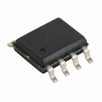
CLOCK EMI REDUCTION SSCG 8-SOIC
Manufacturer
Cypress Semiconductor Corp
Series
Premis™r
Type
Clock/Frequency Synthesizer, Spread Spectrum Clock Generatorr
Datasheet
1.W181-01G.pdf
(9 pages)
Specifications of W181-01G
Pll
Yes
Input
Clock, Crystal
Output
CMOS
Number Of Circuits
1
Ratio - Input:output
1:1
Differential - Input:output
No/No
Frequency - Max
75MHz
Divider/multiplier
Yes/No
Voltage - Supply
3.135 V ~ 5.5 V
Operating Temperature
0°C ~ 70°C
Mounting Type
Surface Mount
Package / Case
8-SOIC (3.9mm Width)
Frequency-max
75MHz
Lead Free Status / RoHS Status
Contains lead / RoHS non-compliant
Other names
428-1395
Available stocks
Company
Part Number
Manufacturer
Quantity
Price
Company:

Part Number:
W181-01G
Manufacturer:
TEXAS
Quantity:
224
Part Number:
W181-01G
Manufacturer:
CYPRESS/赛普拉斯
Quantity:
20 000
Part Number:
W181-01GI
Manufacturer:
CYPRESS/赛普拉斯
Quantity:
20 000
Part Number:
W181-01GT
Manufacturer:
PTC
Quantity:
20 000


Document #: 38-07152 Rev. *D
Pin Definitions
Key Specifications
Supply Voltages: .........................................V
Frequency Range: ............................ 28 MHz ≤ F
Crystal Reference Range.................. 28 MHz ≤ F
Cycle to Cycle Jitter: ....................................... 300 ps (max.)
Selectable Spread Percentage: ................... 1.25% or 3.75%
Output Duty Cycle: ............................... 40/60% (worst case)
Output Rise and Fall Time: .................................. 5 ns (max.)
Table 1. Modulation Width Selection
Table 2. Frequency Range Selection
.................................................................or V
CLKOUT
CLKIN or X1
NC or X2
SSON#
FS1:2
SS%
VDD
GND
NC
Pin Name
FS2
SS%
0
0
1
1
0
1
FS1
W181-01, 02, 03 Output W181-51, 52, 53 Output
0
1
0
1
(Down Spread)
(Down Spread)
8(02/03/52/53)
28 ≤ F
38 ≤ F
46 ≤ F
58 ≤ F
7, 8 (01/51)
Pin No.
–1.25%
–3.75%
(SOIC)
-01, 51
(MHz)
5
1
2
4
6
3
IN
IN
IN
IN
≤ 38
≤ 48
≤ 60
≤ 75
W181 Option#
5, 7, 9, 11, 13,
(TSSOP)(-01)
28 ≤ F
38 ≤ F
-02, 52
Pin No.
(MHz)
12, 1
N/A
N/A
10
14
--
IN
IN
8
2
3
6
4
(Center Spread)
(Center Spread)
≤ 38
≤ 48
±1.875%
±0.625
DD
DD
46 ≤ F
58 ≤ F
Type
= 3.3V ± 5%
Pin
= 5V ± 10%
NC
in
in
O
G
P
-03, 53
I
I
I
I
I
(MHz)
≤ 75 MHz
≤ 40 MHz
N/A
N/A
IN
IN
Output Modulated Frequency: Frequency modulated copy of the
unmodulated input clock (SSON# asserted).
Crystal Connection or External Reference Frequency Input: This pin
has dual functions. It may either be connected to an external crystal, or
to an external reference clock.
Crystal Connection: If using an external reference, this pin must be left
unconnected.
Spread Spectrum Control (Active LOW): Asserting this signal (active
LOW) turns the internal modulation waveform on. This pin has an internal
pull-down resistor.
Frequency Selection Bit(s) 1 and 2: These pins select the frequency
range of operation. Refer to Table 2. These pins have internal pull-up
resistors.
Modulation Width Selection: When Spread Spectrum feature is turned
on, this pin is used to select the amount of variation and peak EMI
reduction that is desired on the output signal. This pin has an internal
pull-up resistor.
Power Connection: Connected to 3.3V or 5V power supply.
Ground Connection: Connect all ground pins to the common system
ground plane.
No Connection
≤ 60
≤ 75
Overview
The W181 products are one series of devices in the Cypress
PREMIS family. The PREMIS family incorporates the latest
advances in PLL spread spectrum frequency synthesizer
techniques. By frequency modulating the output with a
low-frequency carrier, peak EMI is greatly reduced. Use of this
technology allows systems to pass increasingly difficult EMI
testing without resorting to costly shielding or redesign.
In a system, not only is EMI reduced in the various clock lines,
but also in all signals which are synchronized to the clock.
Therefore, the benefits of using this technology increase with
the number of address and data lines in the system. The
Simplified Block Diagram on page 1 shows a simple imple-
mentation.
Functional Description
The W181 uses a phase-locked loop (PLL) to frequency
modulate an input clock. The result is an output clock whose
frequency is slowly swept over a narrow band near the input
signal. The basic circuit topology is shown in Figure 1. The
input reference signal is divided by Q and fed to the phase
detector. A signal from the VCO is divided by P and fed back
to the phase detector also. The PLL will force the frequency of
the VCO output signal to change until the divided output signal
and the divided reference signal match at the phase detector
input. The output frequency is then equal to the ratio of P/Q
times the reference frequency. (Note: For the W181 the output
frequency is equal to the input frequency.) The unique feature
of the Spread Spectrum Frequency Timing Generator is that a
modulating waveform is superimposed at the input to the VCO.
This causes the VCO output to be slowly swept across a
predetermined frequency band.
Pin Description
Page 2 of 9
W181
Related parts for W181-01G
Image
Part Number
Description
Manufacturer
Datasheet
Request
R

Part Number:
Description:
CLOCK EMI REDUCTION SSCG 8-SOIC
Manufacturer:
Cypress Semiconductor Corp
Datasheet:

Part Number:
Description:
Manufacturer:
Cypress Semiconductor Corp
Datasheet:
Part Number:
Description:
Manufacturer:
Cypress Semiconductor Corp
Datasheet:
Part Number:
Description:
Manufacturer:
Cypress Semiconductor Corp
Datasheet:
Part Number:
Description:
Manufacturer:
Cypress Semiconductor Corp
Datasheet:
Part Number:
Description:
Manufacturer:
Cypress Semiconductor Corp
Datasheet: