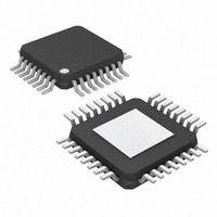
MAX9452EHJ+T Maxim Integrated Products, MAX9452EHJ+T Datasheet - Page 14

MAX9452EHJ+T
Manufacturer Part Number
MAX9452EHJ+T
Description
IC CLOCK GENERATOR W/VCXO 32TQFP
Manufacturer
Maxim Integrated Products
Type
Clock Generatorr
Datasheet
1.MAX9451EHJ.pdf
(18 pages)
Specifications of MAX9452EHJ+T
Pll
Yes
Input
LVCMOS, LVDS, LVPECL
Output
LVDS
Number Of Circuits
1
Ratio - Input:output
2:2
Differential - Input:output
Yes/Yes
Frequency - Max
160MHz
Divider/multiplier
Yes/No
Voltage - Supply
2.4 V ~ 3.6 V
Operating Temperature
-40°C ~ 85°C
Mounting Type
Surface Mount
Package / Case
32-TQFP Exposed Pad, 32-eTQFP, 32-HTQFP, 32-VQFP
Frequency-max
160MHz
Lead Free Status / RoHS Status
Lead free / RoHS Compliant
High-Precision Clock Generators
with Integrated VCXO
Table 8. Control Registers and Control Functions
Table 9. Mapping for the Input Monitor Status
14
CR5, CR6
CR7[1:0] Reserved
CR5[3:2]
CR7[6]
CR7[5]
CR7[4]
CR7[3]
CR7[2]
CR5[7]
CR5[6]
CR5[5]
CR5[4]
CR5[1]
CR5[0]
CR6[7]
CR6[6]
CR6[5]
CR6[4]
CR6[3]
CR6[2]
CR6[1]
CR6[0]
CR7
______________________________________________________________________________________
Status of IN0
Status of IN1
Input clock
selection indicator
LOCK indicator
Holdover status
Output disable
CLK0 enabling
CLK1 enabling
Default input
setting
Input enabling
Revert function
CLK monitor reset C LK m oni tor i s r eset i n r ever t m od e: IN T = 0 and C R7[ 7] = 0, and the P LL sw i tches to the d efaul t i np ut
Holdover function
enabling
Forced holdover
Acquiring nominal
VCXO frequency
Master reset
REF
ODIV select
Acquire select
Reserved
FUNCTION
FUNCTION
0: Normal
1: Failure detected
0: IN0 is currently used
1: IN1 is currently used
1: PLL not locked
0: PLL locked
1: Device is in holdover state
0: Device is in normal state
—
0: Outputs are enabled
1: Outputs disabled to logic-low
0: CLK0 is disabled to high impedance (overrides CR5[7] = 1 setting)
1: CLK0 is enabled
0: CLK1 is disabled to high impedance (overrides CR5[7] = 1 setting)
1: CLK1 is enabled
0: IN0 is the default input
1: IN1 is the default input
00: The selection is controlled by SEL0, SEL1 (see Table 2)
01: Enable IN0, disable IN1
10: Enable IN1, disable IN0
11: Enable both IN0 and IN1
0: The function is not activated
1: The function is activated
0: Holdover function is disabled
1: Holdover function is enabled
0: Holdover is in normal mode
1: Holdover is forced to be activated
As the bit goes from 0 to 1, the current VCXO frequency is taken as the nominal value
As this bit is toggling from 0 to 1, the current VCXO frequency is taking as the nominal holdover
value
The bit acts at the same as the input MR; CR6[4] = 1, the chip is reset
This bit is always set to zero
CR6[2] = 0: DIV0 output drives CLK2
CR6[2] = 1: DIV1 output drives CLK2
CR6[1] = 0 PLL controls the Xtal frequency
CR6[1] = 1 Xtal frequency is controlled by the acquired value (acquired at rising edge of CR6[5])
—
STATE
Table 10. Register Default Values at Power-Up
REGISTER
CR5, CR6
CR0
CR1
CR2
CR3
CR4
CR7
CR8
STATE
P = 1
M = 1
M = 1
N0 = 1
N1 = 1
1. Outputs enable
2. IN0 is the default input
3. Both inputs are enabled by
SEL0 and SEL1
4. Monitor is nonrevertive
5. Holdover is disabled
Status
Reserved
ACTION
CR5: 01100000
CR6: 00000000
DEFAULT
00000000
00000000
00000000
00000000
00000000
00000000
00000000


