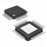
MAX9452EHJ+T Maxim Integrated Products, MAX9452EHJ+T Datasheet

MAX9452EHJ+T
Specifications of MAX9452EHJ+T
Related parts for MAX9452EHJ+T
MAX9452EHJ+T Summary of contents
Page 1
... Gigabit Network Routers and Switches 3G Cellular Phone Base Stations General Jitter Attenuation SPI is a trademark of Motorola, Inc. ________________________________________________________________ Maxim Integrated Products For pricing, delivery, and ordering information, please contact Maxim Direct at 1-888-629-4642, or visit Maxim’s website at www.maxim-ic.com. High-Precision Clock Generators with Integrated VCXO ♦ ...
Page 2
High-Precision Clock Generators with Integrated VCXO ABSOLUTE MAXIMUM RATINGS V to GND ...........................................................-0.3V to +4. GNDA ......................................................-0.3V to +4.0V DDA All Other Pins to GND ...................................-0. Short-Circuit Duration (all pins) ..................................Continuous Continuous Power Dissipation (T ...
Page 3
DC ELECTRICAL CHARACTERISTICS (continued 2.4V to 3.6V, and V DDA DD DDQ V = 3.3V, and V = 1.5V for MAX9451, T DDQ DDQ PARAMETER Output Offset Voltage Change in V Between OS Complementary ...
Page 4
High-Precision Clock Generators with Integrated VCXO 2 SERIAL I C-COMPATIBLE INTERFACE TIMING CHARACTERISTICS ( 2.4V to 3.6V -40°C to +85°C. See Figure 4 for the timing parameters definition.) PARAMETER Serial Clock Bus Free Time Between ...
Page 5
3.3V +25°C, unless otherwise noted.) DD DDA DDQ A V AND V SUPPLY CURRENT DD DDA vs. VOLTAGE (MAX9450 +25° -40° ...
Page 6
High-Precision Clock Generators with Integrated VCXO PIN NAME LOCK Lock Indicator. LOCK goes low when the PLL locks. LOCK is high when the PLL is not locked. 1 INO_ and IN1_ Select Inputs. Drive SEL0 high to activate IN0; drive ...
Page 7
RJ LOCK IN0+ IN0- 0 IN1+ 1 IN1- CMON CLK INT MONITOR SEL0 SEL1 SCL PORT SDA AD0 AD1 SPI PORT GND/CS Detailed Description The MAX9450/MAX9451/MAX9452 clock generators provide high-precision clocks for timing in SONET/SDH systems or ...
Page 8
High-Precision Clock Generators with Integrated VCXO N1 and N2, respectively. CR5 and CR6 are the control function registers for output enabling, reference clock selection, and activation of the clock monitor and the holdover function. CR7 contains the status of clock ...
Page 9
CLKn output, f CLKn is the frequency of the reference clock 32,768) is the dividing factor in the feedback loop 16) are ...
Page 10
High-Precision Clock Generators with Integrated VCXO External Loop Filter When the device switches from one input reference to the other or reverts to an input reference from holdover, the output phase changes smoothly during the transition due to the narrowband ...
Page 11
Data Transfer and Acknowledge Following the START condition, each SCL clock pulse transfers 1 bit. Between a START and a STOP, multiple bytes can be transferred on the 2-wire bus. The first 7 bits (B0–B6) are for the device address. ...
Page 12
High-Precision Clock Generators with Integrated VCXO LOW HIGH SMBCLK SMBDATA t t HD:STA SU:STA A = START CONDITION B = MSB OF ADDRESS CLOCKED INTO SLAVE C = LSB OF ADDRESS CLOCKED INTO SLAVE D = ...
Page 13
Table Address Setting by AD0 and AD1 AD0 AD1 Low Low Low Open Low High Open Low Open Open Open High High Low High Open High High 2 Table and SPI Register Address* ...
Page 14
High-Precision Clock Generators with Integrated VCXO Table 8. Control Registers and Control Functions CR5, CR6 FUNCTION 0: Outputs are enabled CR5[7] Output disable 1: Outputs disabled to logic-low 0: CLK0 is disabled to high impedance (overrides CR5[ setting) ...
Page 15
Table 11. Resistor Value vs. Charge-Pump Current RESISTOR (kΩ 100 150 200 Applications Information Crystal Selection The MAX9450/MAX9451/MAX9452 internal VCXO cir- cuitry requires an external crystal. The frequency of the crystal ranges from 15MHz to 160MHz, depending ...
Page 16
High-Precision Clock Generators with Integrated VCXO (The package drawing(s) in this data sheet may not reflect the most current specifications. For the latest package outline information go to www.maxim-ic.com/packages.) 16 ______________________________________________________________________________________ Package Information PACKAGE OUTLINE, 32L TQFP, 5x5x1.0mm, EP OPTION ...
Page 17
For the latest package outline information go to www.maxim-ic.com/packages.) ______________________________________________________________________________________ High-Precision Clock Generators with Integrated VCXO Package Information (continued) PACKAGE OUTLINE, 32L TQFP, 5x5x1.0mm, EP OPTION ...
Page 18
... Maxim cannot assume responsibility for use of any circuitry other than circuitry entirely embodied in a Maxim product. No circuit patent licenses are implied. Maxim reserves the right to change the circuitry and specifications without notice at any time. 18 ____________________Maxim Integrated Products, 120 San Gabriel Drive, Sunnyvale, CA 94086 408-737-7600 © 2007 Maxim Integrated Products REVISION DESCRIPTION is a registered trademark of Maxim Integrated Products, Inc ...


