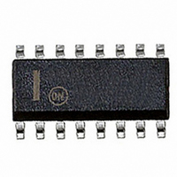
NB2308AI1DR2G ON Semiconductor, NB2308AI1DR2G Datasheet - Page 5

NB2308AI1DR2G
Manufacturer Part Number
NB2308AI1DR2G
Description
IC BUFFER CLK 8OUT 3.3V 16-SOIC
Manufacturer
ON Semiconductor
Type
Zero Delay Bufferr
Datasheet
1.NB2308AI1DR2G.pdf
(12 pages)
Specifications of NB2308AI1DR2G
Pll
Yes with Bypass
Input
Clock
Output
Clock
Number Of Circuits
1
Ratio - Input:output
1:8
Differential - Input:output
No/No
Frequency - Max
133.3MHz
Divider/multiplier
No/No
Voltage - Supply
3 V ~ 3.6 V
Operating Temperature
-40°C ~ 85°C
Mounting Type
Surface Mount
Package / Case
16-SOIC (3.9mm Width)
Frequency-max
133MHz
Lead Free Status / RoHS Status
Lead free / RoHS Compliant
Available stocks
Company
Part Number
Manufacturer
Quantity
Price
Company:
Part Number:
NB2308AI1DR2G
Manufacturer:
ON Semiconductor
Quantity:
1 900
Table 7. SWITCHING CHARACTERISTICS
t
t
t
t
t
t
t
t
t
Parameter
1
1
3
4
5
6
7
J
LOCK
Output Frequency
Duty Cycle = (t
(all devices)
Output Rise Time
(--1, --2, --3, --4)
Output Rise Time
(--1H, --5H)
Output Fall Time
(--1, --2, --3, --4)
Output Fall Time
(--1H, --5H)
Output--to--Output Skew on same Bank
(--1, --2, --3, --4)
Output--to--Output Skew
(--1H, --5H)
Output Bank A--to--Output Bank B Skew
(--1, --4, --5H)
Output Bank A--to--Output Bank B Skew
(--2, --3)
Delay, REF Rising Edge to FBK
Rising Edge
Device--to--Device Skew
Cycle--to--Cycle Jitter
(--1, --1H, --4, --5H)
Cycle--to--Cycle Jitter
(--2, --3)
PLL Lock Time
Description
2
/ t
1
) * 100
V
CC
= 3.0 V to 3.6 V, GND = 0 V, T
http://onsemi.com
30 pF load (all devices)
15 pF load (--1H, --5H)
15 pF load (--1, --2, --3, --4)
Measured at 1.4 V, F
30 pF load
Measured at 1.4 V, F
15 pF load
Measured between 0.8 V and 2.0 V
30 pF load
Measured between 0.8 V and 2.0 V
15 pF load
Measured between 0.8 V and 2.0 V
30 pF load
Measured between 2.0 V and 0.8 V
30 pF load
Measured between 0.8 V and 2.0 V
15 pF load
Measured between 2.0 V and 0.8 V
30 pF load
All outputs equally loaded
All outputs equally loaded
All outputs equally loaded
All outputs equally loaded
Measured at V
Measured at V
device
Measured at 66.67 MHz, loaded outputs,
15 pF load
Measured at 66.67 MHz, loaded outputs,
30 pF load
Measured at 133.3 MHz, loaded outputs
15 pF load
Measured at 66.67 MHz, loaded outputs,
30 pF load
Measured at 66.67 MHz, loaded outputs,
15 pF load
Stable power supply, valid clock presented
on REF and FBK pins
5
Test Conditions
DD
DD
/2
/2 on the FBK pins of the
OUT
OUT
= < 66.66 MHz
= < 50 MHz
A
= --40C to +85C
40.0
45.0
Min
15
15
15
50.0
50.0
Typ
0
0
133.3
133.3
250
Max
60.0
55.0
2.20
1.50
1.50
2.20
1.50
1.25
100
200
200
200
400
700
200
200
100
400
400
1.0
MHz
Unit
ms
ns
ns
ps
ps
ps
ps
%


