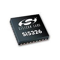
SI5326A-C-GM Silicon Laboratories Inc, SI5326A-C-GM Datasheet - Page 60

SI5326A-C-GM
Manufacturer Part Number
SI5326A-C-GM
Description
IC ANY-RATE MULTI/ATTEN 36-QFN
Manufacturer
Silicon Laboratories Inc
Type
Clock Multiplierr
Datasheet
1.SI5326B-C-GM.pdf
(72 pages)
Specifications of SI5326A-C-GM
Package / Case
36-QFN
Pll
Yes
Input
Clock
Output
CML, CMOS, LVDS, LVPECL
Number Of Circuits
1
Ratio - Input:output
2:2
Differential - Input:output
Yes/Yes
Frequency - Max
1.4GHz
Divider/multiplier
Yes/Yes
Voltage - Supply
1.71 V ~ 3.63 V
Operating Temperature
-40°C ~ 85°C
Mounting Type
Surface Mount
Frequency-max
1.4GHz
Max Input Freq
710 MHz
Max Output Freq
945 MHz
Maximum Operating Temperature
+ 85 C
Minimum Operating Temperature
- 40 C
Mounting Style
SMD/SMT
Number Of Outputs
2
Supply Current
251 mA
Supply Voltage (max)
3.3 V
Supply Voltage (min)
1.8 V
Lead Free Status / RoHS Status
Lead free / RoHS Compliant
Lead Free Status / RoHS Status
Lead free / RoHS Compliant, Lead free / RoHS Compliant
Available stocks
Company
Part Number
Manufacturer
Quantity
Price
Part Number:
SI5326A-C-GMR
Manufacturer:
SILICON LABS/芯科
Quantity:
20 000
Si5326
60
Note: Internal register names are indicated by underlined italics, e.g., INT_PIN. See Section “5.Register Map”.
Pin #
18
19
20
Pin Name
DEC
LOL
INC
I/O
O
I
I
Signal Level
LVCMOS
LVCMOS
LVCMOS
PLL Loss of Lock Indicator.
This pin functions as the active high PLL loss of lock indicator if the
LOL_PIN register bit is set to 1.
0 = PLL locked
1 = PLL unlocked
If LOL_PIN = 0, this pin will tristate. Active polarity is controlled by
the LOL_POL bit. The PLL lock status will always be reflected in the
LOL_INT read only register bit.
Skew Decrement.
A pulse on this pin decreases the input to output device skew by
1/f
skew adjustment by this method.
Pin control is enabled by setting INCDEC_PIN = 1. If
INCDEC_PIN = 0, this pin is ignored and output skew is controlled
via the CLAT register.
If both INC and DEC are tied high, phase buildout is disabled and
the device maintains a fixed-phase relationship between the
selected input clock and the output clock during an input clock
switch.
See the Si53xx Family Reference Manual for more details.
This pin has a weak pull-down.
Skew Increment.
A pulse on this pin increases the input to output device skew by
1/f
skew adjustment by this method.
Pin control is enabled by setting INCDEC_PIN = 1. If
INCDEC_PIN = 0, this pin is ignored and output skew is controlled
via the CLAT register.
If both INC and DEC are tied high, phase buildout is disabled and
the device maintains a fixed-phase relationship between the
selected input clock and the output clock during an input clock
switch.
See the Si53xx Family Reference Manual for more details.
Note: INC does not increase skew if NI_HS = 4.
This pin has a weak pull-down.
OSC
OSC
(approximately 200 ps). There is no limit on the range of
(approximately 200 ps). There is no limit on the range of
Rev. 1.0
Description


