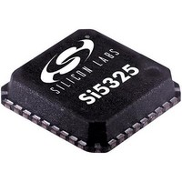
SI5325C-C-GM Silicon Laboratories Inc, SI5325C-C-GM Datasheet - Page 9

SI5325C-C-GM
Manufacturer Part Number
SI5325C-C-GM
Description
IC UP-PROG CLK MULTIPLIER 36-QFN
Manufacturer
Silicon Laboratories Inc
Type
Clock Multiplierr
Datasheet
1.SI5325C-C-GM.pdf
(52 pages)
Specifications of SI5325C-C-GM
Number Of Circuits
1
Package / Case
36-QFN
Pll
Yes
Input
Clock
Output
CML, CMOS, LVDS, LVPECL
Ratio - Input:output
2:2
Differential - Input:output
Yes/Yes
Frequency - Max
346MHz
Divider/multiplier
Yes/Yes
Voltage - Supply
1.71 V ~ 3.63 V
Operating Temperature
-40°C ~ 85°C
Mounting Type
Surface Mount
Frequency-max
346MHz
Maximum Input Frequency
710 MHz
Minimum Input Frequency
10 MHz
Output Frequency Range
10 MHz to 346 MHz
Supply Voltage (max)
3.63 V
Supply Voltage (min)
1.71 V
Maximum Operating Temperature
+ 85 C
Minimum Operating Temperature
- 40 C
Mounting Style
SMD/SMT
Operating Supply Voltage
1.8 V, 2.5 V, 3.3 V
Lead Free Status / RoHS Status
Lead free / RoHS Compliant
Available stocks
Company
Part Number
Manufacturer
Quantity
Price
Part Number:
SI5325C-C-GM
Manufacturer:
SILICONLABS/芯科
Quantity:
20 000
2. Pin Descriptions: Si5325
Pin numbers are preliminary and subject to change.
2, 7, 9, 14,
Note: Internal register names are indicated by underlined italics, e.g., INT_PIN. See Si5325 Register Map.
18, 30, 33
Pin #
1
3
Pin Name
INT_C1B
RST
NC
I/O
O
I
INT_C1B
Table 3. Si5325 Pin Descriptions
Signal Level
GND
GND
VDD
RST
C2B
NC
NC
NC
LVCMOS
LVCMOS
1
2
3
4
5
6
7
8
9
36
10 11 12 13 14 15 16 17
Preliminary Rev. 0.4
35
34
33
External Reset.
Active low input that performs external hardware reset of
device. Resets all internal logic to a known state and forces
the device registers to their default value. Clock outputs are
tristated during reset. The part must be programmed after a
reset or power-on to get a clock output. See Family Refer-
ence Manual for details.
This pin has a weak pull-up.
No Connect.
This pin must be left unconnected for normal operation.
Interrupt/CKIN1 Invalid Indicator.
This pin functions as a device interrupt output or an alarm
output for CKIN1. If used as an interrupt output, INT_PIN
must be set to 1. The pin functions as a maskable interrupt
output with active polarity controlled by the INT_POL register
bit.
If used as an alarm output, the pin functions as a LOS (and
optionally FOS) alarm indicator for CKIN1. Set
CK1_BAD_PIN = 1 and INT_PIN = 0.
0 = CKIN1 present.
1 = LOS (FOS) on CKIN1.
The active polarity is controlled by CK_BAD_POL. If no func-
tion is selected, the pin tristates.
GND
Pad
32
31
30
29
28
18
27
26
25
24
23
22
21
20
19
SDI
A2_SS
A1
A0
SDA_SDO
SCL
CS_CA
GND
GND
Description
Si5325
9


