CY7B991V-5JI Cypress Semiconductor Corp, CY7B991V-5JI Datasheet
CY7B991V-5JI
Specifications of CY7B991V-5JI
Available stocks


Related parts for CY7B991V-5JI


CY7B991V-5JI Summary of contents
Page 1
... Cypress Semiconductor Corporation Document Number: 38-07138 Rev. *E Programmable Skew Clock Buffer Functional Description The CY7B991 and CY7B992 Programmable Skew Clock Buffers (PSCB) offer user selectable control over system clock functions. These multiple output clock drivers provide the system integrator with functions necessary to optimize the timing of high perfor- mance computer systems ...
Page 2
Contents Features ................................................................................1 Functional Description ........................................................1 Logic Block Diagram ...........................................................1 Contents ...............................................................................2 Pinouts .................................................................................3 Block Diagram Description .................................................4 Phase Frequency Detector and Filter .............................4 VCO and Time Unit Generator .......................................4 Skew Select Matrix .........................................................4 Test Mode .............................................................................5 Maximum Ratings ................................................................6 ...
Page 3
Pinouts Figure 1. Pin Configuration – 32-Pin PLCC/LCC Package Table 1. Pin Definition Signal Name IO REF I Reference frequency input. This input supplies the frequency and timing against which all functional variations are measured PLL feedback input ...
Page 4
Block Diagram Description Phase Frequency Detector and Filter The Phase Frequency Detector and Filter blocks accept inputs from the reference frequency (REF) input and the feedback (FB) input and generate correction information to control the frequency of the Voltage Controlled ...
Page 5
Figure 2 shows the typical outputs with FB connected to a zero skew output. Figure 2. Typical Outputs with FB Connected to a Zero-Skew Output FBInput REFInput 1Fx 3Fx 2Fx 4Fx (N/A) LM – – 4t ...
Page 6
Maximum Ratings Exceeding maximum ratings may shorten the useful life of the device. User guidelines are not tested. Storage Temperature ................................. –65 Ambient Temperature with Power Applied ............................................ –55 Supply Voltage to Ground Potential................–0.5V to +7.0V DC Input Voltage ............................................–0.5V ...
Page 7
Electrical Characteristics [6] Over the Operating Range Parameter Description V Output HIGH Voltage OH V Output LOW Voltage OL V Input HIGH Voltage IH (REF and FB inputs only) V Input LOW Voltage IL (REF and FB inputs only) V ...
Page 8
Capacitance CMOS output buffer current and power dissipation specified at 50 MHz reference frequency. Parameter Description C Input Capacitance IN 5V R1=130 R1 R2= (Includes fixture and probe capacitance TTL AC ...
Page 9
Switching Characteristics [2, 13] Over the Operating Range Parameter Description f Operating Clock NOM Frequency in MHz t REF Pulse Width HIGH RPWH t REF Pulse Width LOW RPWL t Programmable Skew Unit U t Zero Output Matched-Pair Skew SKEWPR ...
Page 10
Switching Characteristics [2, 13] Over the Operating Range (continued) Parameter Description f Operating Clock NOM Frequency in MHz t REF Pulse Width HIGH RPWH t REF Pulse Width LOW RPWL t Programmable Skew Unit U t Zero Output Matched-Pair Skew ...
Page 11
Switching Characteristics [2, 13] Over the Operating Range (continued) Parameter Description f Operating Clock NOM Frequency in MHz t REF Pulse Width HIGH RPWH t REF Pulse Width LOW RPWL t Programmable Skew Unit U t Zero Output Matched-Pair Skew ...
Page 12
AC Timing Diagrams REF OTHER Q INVERTED Q t SKEW3,4 REF DIVIDED SKEW1,3, 4 REF DIVIDED BY 4 Document Number: 38-07138 Rev REF RPWL t RPWH t ODCV t ODCV ...
Page 13
Operational Mode Descriptions Figure 4. Zero Skew and Zero Delay Clock Driver FB SYSTEM REF CLOCK FS 4F0 4F1 3F0 3F1 2F0 2F1 1F0 1F1 TEST Figure 4 shows the PSCB configured as a zero skew clock buffer. In this ...
Page 14
FB and REF inputs and aligns their rising edges to ensure that all outputs have precise phase alignment. Clock skews are advanced by ±6 time units (tU) when using an output selected for zero skew as the feedback. A ...
Page 15
MHz. Figure 9 shows some of the functions that are selectable on the 3Qx and 4Qx outputs. These include inverted outputs and outputs that offer divide-by-2 and divide-by-4 timing. An ...
Page 16
FB SYSTEM REF CLOCK FS 4F0 4F1 3F0 3F1 2F0 2F1 1F0 1F1 TEST Figure 10 shows the CY7B991 and 992 connected in series to construct a zero skew clock distribution tree between boards. Delays of the downstream clock buffers ...
Page 17
Ordering Information Accuracy Ordering Code (ps) 250 CY7B991–2JC 32-Pin Plastic Leaded Chip Carrier CY7B991–2JCT 32-Pin Plastic Leaded Chip Carrier - Tape and Reel 500 CY7B991–5JC 32-Pin Plastic Leaded Chip Carrier CY7B991–5JCT 32-Pin Plastic Leaded Chip Carrier - Tape and Reel ...
Page 18
Military Specifications Group A Subgroup Testing DC Characteristics Parameter Subgroups IHH IMM ...
Page 19
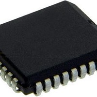
Package Diagrams (continued) Document Number: 38-07138 Rev. *E Figure 11. 32-Pin Plastic Leaded Chip Carrier CY7B991 CY7B992 51-85002 *C Page [+] Feedback ...
Page 20
... Cypress against all charges. Any Source Code (software and/or firmware) is owned by Cypress Semiconductor Corporation (Cypress) and is protected by and subject to worldwide patent protection (United States and foreign), United States copyright laws and international treaty provisions. Cypress hereby grants to licensee a personal, non-exclusive, non-transferable license to copy, use, modify, create derivative works of, and compile the Cypress Source Code and derivative works for the sole purpose of creating custom software and or firmware in support of licensee product to be used only in conjunction with a Cypress integrated circuit as specified in the applicable agreement ...