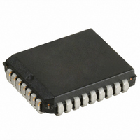
CY7B991V-7JC Cypress Semiconductor Corp, CY7B991V-7JC Datasheet

CY7B991V-7JC
Specifications of CY7B991V-7JC
Available stocks
Related parts for CY7B991V-7JC
CY7B991V-7JC Summary of contents
Page 1
... Operates from a single 3.3V supply • Low operating current • 32-pin PLCC package • Jitter < 200 ps peak-to-peak (< RMS) Functional Description The CY7B991V Low Voltage Programmable Skew Clock Buff- er (LVPSCB) offers user-selectable control over system clock Logic Block Diagram TEST PHASE ...
Page 2
... HIGH U 22.7 HIGH 38.5 HIGH 62.5 , LOW indicates a connection to GND, and MID indicates an open connection. Internal termination CC / the V NOM CY7B991V 3.3V RoboClock Output Functions 1F0, 2F0, 1Q0, 1Q1, 3F0, 4F0 2Q0, 2Q1 3Q0, 3Q1 LOW –4t Divide by 2 Divide MID – ...
Page 3
... Figure 1. Typical Outputs with FB Connected to a Zero-Skew Output Test Mode The TEST input is a three-level input. In normal system oper- ation, this pin is connected to ground, allowing the CY7B991V to operate as explained briefly above (for testing purposes, any of the three-level inputs can have a removable jumper to ground tied LOW through a 100 resistor ...
Page 4
... CY7B991V should be tested one output at a time, output shorted for less than one second, less than 10% duty cycle. Room temperature only. 8. Total output current per output pair can be approximated by the following expression that includes device current plus load current: CY7B991V [(4 + 0.11F) + [((835 – ...
Page 5
... Jitter Notes: 11. Test measurement levels for the CY7B991V are TTL levels (1.5V to 1.5V). Test conditions assume signal transition times less and output loading as shown in the AC Test Loads and Waveforms unless otherwise specified. 12. Guaranteed by statistical correlation. Tested initially and after any design or process changes that may affect these parameters. ...
Page 6
... Document #: 38-07141 Rev. ** [2, 11] (continued) Description [ LOW [ MID [ HIGH [13, 14] [13, 15] [13, 17] [13, 17] [13, 17] [13, 17] [12, 18] [19] [20] [20] [12] RMS [12] Peak-to-Peak CY7B991V 3.3V RoboClock CY7B991V–5 Min. Typ. Max. Unit 15 30 MHz 5.0 ns 5.0 ns See Table 1 0.1 0.25 ns 0.25 0.5 ns 0.6 0.7 ns ...
Page 7
... Document #: 38-07141 Rev. ** [2, 11] (continued) Description [ LOW [ MID [ HIGH [13, 14] [13, 15] [13, 17] [13, 17] [13, 17] [13, 17] [12, 18] [19] [20] [20] [12] RMS [12] Peak-to-Peak CY7B991V 3.3V RoboClock CY7B991V–7 Min. Typ. Max. Unit 15 30 MHz 5.0 ns 5.0 ns See Table 1 0.1 0.25 ns 0.3 0.75 ns 0.6 1 ...
Page 8
... AC Timing Diagrams t REF t RPWH REF SKEWPR, t SKEW0,1 OTHER Q INVERTED Q t SKEW3,4 REF DIVIDED SKEW1,3, 4 REF DIVIDED BY 4 Document #: 38-07141 Rev RPWL t ODCV t ODCV t SKEWPR, t SKEW0,1 t SKEW2 t SKEW2 t SKEW3,4 t SKEW3,4 t SKEW2,4 CY7B991V 3.3V RoboClock t JR 7B991V–8 Page ...
Page 9
... Figure 2. Zero-Skew and/or Zero-Delay Clock Driver Figure 2 shows the LVPSCB configured as a zero-skew clock buffer. In this mode the CY7B991V can be used as the basis for a low-skew clock distribution tree. When all of the function select inputs (xF0, xF1) are left open, the outputs are aligned and may each drive a terminated transmission line to an inde- pendent load ...
Page 10
... It can multiply by two and four or divide by two (and four) at the same time that it is shifting its outputs over a wide range or maintaining zero skew between selected outputs. CY7B991V 3.3V RoboClock frequency outputs without concern for ris- REF ...
Page 11
... TEST Figure 8 shows the CY7B991V connected in series to con- struct a zero-skew clock distribution tree between boards. De- lays of the downstream clock buffers can be programmed to compensate for the wire length (i.e., select negative skew equal to the wire delay) necessary to connect them to the mas- Document #: 38-07141 Rev ...
Page 12
... Package Type J65 32-Lead Plastic Leaded Chip Carrier J65 32-Lead Plastic Leaded Chip Carrier J65 32-Lead Plastic Leaded Chip Carrier J65 32-Lead Plastic Leaded Chip Carrier 32-Lead Plastic Leaded Chip Carrier CY7B991V 3.3V RoboClock Operating Range Commercial Commercial Industrial Commercial Page ...
Page 13
... Document Title: CY7B991V 3.3V RoboClock Low Voltage Programmable Skew Clock Buffer Document Number: 38-07141 Issue REV. ECN NO. Date ** 110250 12/17/01 Document #: 38-07141 Rev. ** Orig. of Change Description of Change SZV Change from Spec number: 38-00641 to 38-07141 CY7B991V 3.3V RoboClock Page ...


