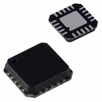
ADF4108BCPZ Analog Devices Inc, ADF4108BCPZ Datasheet

ADF4108BCPZ
Specifications of ADF4108BCPZ
Available stocks
Related parts for ADF4108BCPZ
ADF4108BCPZ Summary of contents
Page 1
FEATURES 8.0 GHz bandwidth 3 3.6 V power supply Separate charge pump supply (V ) allows extended tuning P voltage in 3.3 V systems Programmable, dual-modulus prescaler 8/9, 16/17, 32/33, or 64/65 Programmable charge pump currents Programmable antibacklash ...
Page 2
ADF4108 TABLE OF CONTENTS Features .............................................................................................. 1 Applications....................................................................................... 1 General Description ......................................................................... 1 Functional Block Diagram .............................................................. 1 Revision History ............................................................................... 2 Specifications..................................................................................... 3 Timing Characteristics ................................................................ 5 Absolute Maximum Ratings............................................................ 6 ESD Caution.................................................................................. 6 Pin Configuration and Function Descriptions............................. ...
Page 3
SPECIFICATIONS 3.3 V ± 2%, AV ≤ unless otherwise noted. MAX Table 1. Parameter B Version RF CHARACTERISTICS RF Input Frequency (RF ) 1.0/8 Input Sensitivity −5/+5 ...
Page 4
ADF4108 Parameter NOISE CHARACTERISTICS 9 Normalized Phase Noise Floor 10 Phase Noise Performance 11 7900 MHz Output Spurious Signals 7900 MHz Output 11 1 Operating temperature range (B version) is −40°C to +85°C. 2 The B chip specifications are given ...
Page 5
TIMING CHARACTERISTICS 3.3 V ± 2%, AV ≤ unless otherwise noted. MAX Table 2. 1 Parameter Limit ...
Page 6
ADF4108 ABSOLUTE MAXIMUM RATINGS T = 25°C, unless otherwise noted. A Table 3. Parameter GND GND Digital I/O Voltage to GND Analog I/O ...
Page 7
PIN CONFIGURATION AND FUNCTION DESCRIPTIONS Table 4. Pin Function Descriptions Pin No. Mnemonic Description 1 CPGND Charge Pump Ground. This is the ground return path for the charge pump AGND Analog Ground. This is the ground return path ...
Page 8
ADF4108 TYPICAL PERFORMANCE CHARACTERISTICS FREQ UNIT: GHz KEYWORD: R PARAM TYPE: s DATA FORMAT: MA Freq MAGS11 ANGS11 Freq 4.30000 0.50000 0.89148 –17.2820 0.88133 –20.6919 4.40000 0.60000 0.70000 0.87152 –24.5386 4.50000 0.80000 0.85855 –27.3228 4.60000 0.90000 0.84911 –31.0698 4.70000 1.00000 ...
Page 9
THEORY OF OPERATION REFERENCE INPUT STAGE The reference input stage is shown in Figure 10. SW1 and SW2 are normally closed switches. SW3 is normally open. When power-down is initiated, SW3 is closed and SW1 and SW2 are opened. This ...
Page 10
ADF4108 PHASE FREQUENCY DETECTOR AND CHARGE PUMP The phase frequency detector (PFD) takes inputs from the R counter and N counter ( and produces an output proportional to the phase and frequency difference between them. Figure ...
Page 11
LATCH SUMMARY ANTI- TEST BACKLASH RESERVED MODE BITS WIDTH DB23 DB22 DB21 DB20 DB19 DB18 DB17 DB16 DB15 DB14 DB13 DB12 DB11 DB10 LDP T2 T1 ABP2 RESERVED DB23 DB22 DB21 DB20 DB19 DB18 DB17 DB16 DB15 ...
Page 12
ADF4108 REFERENCE COUNTER LATCH MAP TEST BACKLASH RESERVED MODE BITS DB23 DB22 DB21 DB20 DB19 DB18 DB17 DB16 DB15 DB14 DB13 DB12 DB11 DB10 0 0 LDP T2 T1 ABP2 DON’T CARE ABP2 ...
Page 13
AB COUNTER LATCH MAP RESERVED DB23 DB22 DB21 DB20 DB19 DB18 DB17 B13 B12 B11 B10 X = DON’T CARE B13 B12 B11 ...
Page 14
ADF4108 FUNCTION LATCH MAP CURRENT CURRENT PRESCALER SETTING SETTING VALUE 2 DB23 DB22 DB21 DB20 DB19 DB18 DB17 DB16 DB15 DB14 DB13 DB12 DB11 DB10 P2 P1 PD2 CPI6 CPI5 CPI4 CPI3 CPI2 TC4 ...
Page 15
INITIALIZATION LATCH MAP CURRENT CURRENT PRESCALER SETTING SETTING VALUE 2 DB23 DB22 DB21 DB20 DB19 DB18 DB17 DB16 DB15 DB14 DB13 DB12 DB11 DB10 P2 P1 PD2 CPI6 CPI5 CPI4 CPI3 CPI2 TC4 ...
Page 16
ADF4108 FUNCTION LATCH The on-chip function latch is programmed with C2 and C1 set to 1 and 0, respectively. Figure 18 shows the input data format for programming the function latch. Counter Reset DB2 (F1) is the counter reset bit. ...
Page 17
Charge Pump Currents CPI3, CPI2, and CPI1 program Current Setting 1 for the charge pump. CPI6, CPI5, and CPI4 program Current Setting 2 for the charge pump. The truth table is given in Figure 18. Prescaler Value P2 and P1 ...
Page 18
ADF4108 INTERFACING The ADF4108 has a simple SPI-compatible serial interface for writing to the device. CLK, DATA, and LE control the data transfer. When LE (latch enable) goes high, the 24 bits that have been clocked into the input register ...
Page 19
PCB DESIGN GUIDELINES FOR CHIP SCALE PACKAGE The lands on the chip scale package (CP-20-1) are rectangular. The printed circuit board pad for these should be 0.1 mm longer than the package land length and 0.05 mm wider than the ...
Page 20
... Model Temperature Range 1 ADF4108BCPZ −40°C to +85°C 1 ADF4108BCPZ-RL −40°C to +85°C 1 ADF4108BCPZ-RL7 −40°C to +85°C 1 EVAL-ADF4108EBZ1 RoHS Compliant Part. ©2006–2007 Analog Devices, Inc. All rights reserved. Trademarks and registered trademarks are the property of their respective owners. D06015-0-12/07(A) ...


