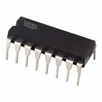
74HCT9046AN,112 NXP Semiconductors, 74HCT9046AN,112 Datasheet - Page 11

74HCT9046AN,112
Manufacturer Part Number
74HCT9046AN,112
Description
IC PLL W/BAND GAP VCO 16-DIP
Manufacturer
NXP Semiconductors
Type
Phase Lock Loop (PLL)r
Series
74HCTr
Datasheet
1.74HCT9046AD118.pdf
(43 pages)
Specifications of 74HCT9046AN,112
Number Of Circuits
1
Package / Case
16-DIP (0.300", 7.62mm)
Pll
Yes
Input
Clock
Output
Clock
Ratio - Input:output
2:2
Differential - Input:output
No/No
Frequency - Max
16MHz
Divider/multiplier
No/No
Voltage - Supply
4.5 V ~ 5.5 V
Operating Temperature
-40°C ~ 125°C
Mounting Type
Through Hole
Frequency-max
16MHz
Supply Voltage (max)
5.5 V
Supply Voltage (min)
4.5 V
Maximum Operating Temperature
+ 125 C
Minimum Operating Temperature
- 40 C
Mounting Style
SMD/SMT
Operating Supply Voltage
4.5 V to 5.5 V
Lead Free Status / RoHS Status
Lead free / RoHS Compliant
Lead Free Status / RoHS Status
Lead free / RoHS Compliant, Lead free / RoHS Compliant
Other names
568-2913-5
935044170112
935044170112
NXP Semiconductors
74HCT9046A_6
Product data sheet
Fig 10. Timing diagram for PC2
The pulse overlap of the up and down signals (typically 15 ns).
SIG_IN
UP
DOWN
CURRENT AT
PC2_OUT
PC2_OUT/VCO_IN
PCP_OUT
COMP_IN
VCO_OUT
When the frequency of SIG_IN is higher than that of COMP_IN, the source output driver is
held ‘ON’ for most of the input signal cycle time and for the remainder of the cycle time
both drivers are ‘OFF’ (3-state). If the SIG_IN frequency is lower than the COMP_IN
frequency, then it is the sink driver that is held ‘ON’ for most of the cycle. Subsequently the
voltage at the capacitor (C2) of the low-pass filter connected to PC2_OUT varies until the
signal and comparator inputs are equal in both phase and frequency. At this stable point
the voltage on C2 remains constant as the PC2 output is in 3-state and the VCO input at
pin 9 is a high-impedance. Also in this condition the signal at the phase comparator pulse
output (PCP_OUT) has a minimum output pulse width equal to the overlap time, so can be
used for indicating a locked condition.
Thus for PC2 no phase difference exists between SIG_IN and COMP_IN over the full
frequency range of the VCO. Moreover, the power dissipation due to the low-pass filter is
reduced because both output drivers are OFF for most of the signal input cycle. It should
be noted that the PLL lock range for this type of phase comparator is equal to the capture
range and is independent of the low-pass filter. With no signal present at SIG_IN the VCO
adjust, via PC2, to its lowest frequency.
By using current sources as charge pump output on PC2, the dead zone or backlash time
could be reduced to zero. Also, the pulse widening due to the parasitic output capacitance
plays no role here. This enables a linear transfer function, even in the vicinity of the zero
crossing. The differences between a voltage switch charge pump and a current switch
charge pump are shown in
PC_IN
Rev. 06 — 15 September 2009
high-impedance OFF-state,
(zero current)
Figure
11.
PLL with band gap controlled VCO
74HCT9046A
15 ns typical
mbd047
© NXP B.V. 2009. All rights reserved.
11 of 43


