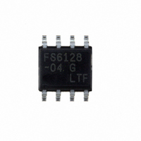
FS6128-04G-XTD ON Semiconductor, FS6128-04G-XTD Datasheet - Page 4

FS6128-04G-XTD
Manufacturer Part Number
FS6128-04G-XTD
Description
IC CLOCK GEN PLL W/VCXO 8-SOIC
Manufacturer
ON Semiconductor
Type
PLL Clock Generatorr
Datasheet
1.FS6128-04G-XTD.pdf
(6 pages)
Specifications of FS6128-04G-XTD
Pll
Yes
Input
Crystal
Output
Clock
Number Of Circuits
1
Ratio - Input:output
1:1
Differential - Input:output
No/No
Frequency - Max
27MHz
Divider/multiplier
Yes/No
Voltage - Supply
3 V ~ 3.6 V
Operating Temperature
0°C ~ 70°C
Mounting Type
Surface Mount
Package / Case
8-SOIC (3.9mm Width)
Frequency-max
27MHz
Mounting Style
SMD/SMT
Max Input Freq
13.5 MHz
Max Output Freq
27 MHz
Number Of Outputs
1
Operating Supply Voltage
3.3 V
Operating Temperature Range
0 C to + 70 C
Supply Current
30 mA
Lead Free Status / RoHS Status
Lead free / RoHS Compliant
Other names
766-1021
Available stocks
Company
Part Number
Manufacturer
Quantity
Price
Company:
Part Number:
FS6128-04G-XTD
Manufacturer:
MICREL
Quantity:
179
FS6128-04
Table 5: DC Electrical Specifications
Note: Unless otherwise stated V
asterisk (*) represent nominal characterization data and are not production tested to any specific limits. Where given, MIN and MAX characterization
data are ±3σ from typical. Negative currents indicate current flows out of the device.
Table 6: AC Timing Specifications
Note: Unless otherwise stated, V
asterisk (*) represent nominal characterization data and are not production tested to any specific limits. Where given, MIN and MAX characterization
data are ±3σ from typical.
Parameter
Overall
Supply current, dynamic, with loaded outputs
Supply current, static
Voltage-Controlled Crystal Oscillator (contact factory for approved crystal sources or other application assistance)
Crystal loading capacitance at center tuning
voltage
Crystal resonator motional capacitance
XTUNE effective range
Synthesized load capacitance min.
Synthesized load capacitance max.
VCXO tuning range
VCXO tuning characteristic
Crystal drive level
Clock Output (CLK)
High-level output source current*
Low-level output sink current*
Output impedance*
Short circuit source current*
Short circuit sink current*
Parameter
Overall
VCXO stabilization time*
PLL stabilization time*
Synthesis error
Clock Output (CLK)
Duty cycle*
Jitter, period (peak-peak)*
Jitter, long term (σγ(τ)
Rise time*
Fall time*
Symbol
t
t
t
t
t
t
DD
VCXOSTB
PLLSTB
j(ΔP)
j(LT)
r
f
DD
= 3.3V ±10% no load on any output and ambient temperature range T
= 3.3V ±10%, no load on any output, and ambient temperature range T
Conditions/Descriptions
From power valid
From VCXO stable
(Unless otherwise noted in frequency table)
Ratio of high pulse width (as measured from rising edge to next
falling edge at V
From rising edge to next rising edge at V
From 0-500μs at V
V
V
DD
DD
= 3.3V; V
= 3.3V; V
Symbol
I
I
C
C
C
C
I
I
Z
Z
I
I
DD
DD
OH
OL
OSH
OSL
OH
OL
L(xtal)
1
L1
L2
Rev. 2 | Page 4 of 6 | www.onsemi.com
O
O
= 0.3V to 3.0V; C
= 3.0V to 0.3V; C
DD
/2) to one clock period
DD
Conditions/Descriptions
f
XIN = 0V; VDD = 3.6V
Order crystal for this capacitance
(parallel load) at desired center
frequency
Specified motional capacitance of the
crystal will affect pullability (see text)
@V(XTUNE) = minimum value
@V(XTUNE) = maximum value
f
= 25fF (peak-to-peak)
Note: positive change of XTUNE =
positive change of VCXO frequency
R
V
V
V
V
V
V
/2, CL = 10pF compared to ideal clock source
XAL
XTAL
O
O
O
O
O
O
XTAL
= 2.0V
= 0.4V
= 0.1V
= 0.1V
= 0V; shorted for 30s, max.
= 3.3V; shorted for 30s, max.
= 13.5MHz; CL = 10pF; VDD = 3.6V
= 13.5MHz; C
= 20Ω; C
DD
DD
; output driving high
; output driving low
L
L
= 10pF
= 10pF
L
= 20pF
L(xtal)
DD
/2, CL = 10pF 200 ps
= 14pF; C
1
(xtal)
A
A
= 0°C to 70°C. Parameters denoted with an
= 0°C to 70°C. Parameters denoted with an
Min.
0
Min.
45
Typ.
300
150
200
-40
-55
30
14
25
10
20
17
25
25
55
3
Typ.
100
200
100
1.7
1.7
10
0
Max.
3
Max.
55
ppm/V
Units
ppm
mA
mA
μW
mA
mA
mA
mA
Units
pF
pF
pF
fF
Ω
ppm
V
ms
μs
ps
ps
ns
ns
%


