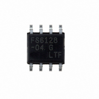
FS6128-04G-XTD ON Semiconductor, FS6128-04G-XTD Datasheet - Page 2

FS6128-04G-XTD
Manufacturer Part Number
FS6128-04G-XTD
Description
IC CLOCK GEN PLL W/VCXO 8-SOIC
Manufacturer
ON Semiconductor
Type
PLL Clock Generatorr
Datasheet
1.FS6128-04G-XTD.pdf
(6 pages)
Specifications of FS6128-04G-XTD
Pll
Yes
Input
Crystal
Output
Clock
Number Of Circuits
1
Ratio - Input:output
1:1
Differential - Input:output
No/No
Frequency - Max
27MHz
Divider/multiplier
Yes/No
Voltage - Supply
3 V ~ 3.6 V
Operating Temperature
0°C ~ 70°C
Mounting Type
Surface Mount
Package / Case
8-SOIC (3.9mm Width)
Frequency-max
27MHz
Mounting Style
SMD/SMT
Max Input Freq
13.5 MHz
Max Output Freq
27 MHz
Number Of Outputs
1
Operating Supply Voltage
3.3 V
Operating Temperature Range
0 C to + 70 C
Supply Current
30 mA
Lead Free Status / RoHS Status
Lead free / RoHS Compliant
Other names
766-1021
Available stocks
Company
Part Number
Manufacturer
Quantity
Price
Company:
Part Number:
FS6128-04G-XTD
Manufacturer:
MICREL
Quantity:
179
FS6128-04
Table 1: Crystal / Output Frequencies
Note: Contact ON Semiconductor for custom PLL frequencies.
Table 2: Pin Descriptions
Key: AI = Analog Input; AO = Analog Output; DI = Digital Input; DI
Input/Output; DI-3 = Three-Level Digital Input, DO = Digital Output; P = Power/Ground; # = Active Low Pin
3.0 Functional Block Diagram
3.1 Voltage-Controlled Crystal Oscillator (VCXO)
The VCXO provides a tunable, low-jitter frequency reference for the rest of the FS6128 system components. Loading capacitance for
the crystal is internal to the FS6128. No external components (other than the resonator itself) are required for operation of the VCXO.
Continuous fine-tuning of the VCXO frequency is accomplished by varying the voltage on the XTUNE pin. The value of this voltage
controls the effective capacitance presented to the crystal. The actual amount that this load capacitance change will alter the oscillator
frequency depends on the characteristics of the crystal as well as the oscillator circuit itself.
It is important that the crystal load capacitance is specified correctly to “center” the tuning range. See Table 5.
Device
FS128-04
Pin
1
2
3
4
5
6
7
8
Type
AI
P
AI
P
DO
-
DO
AO
f
13.500
XIN
(MHz)
Name
XIN
VDD
XTUNE
VSS
CLK
n/c
VSS
XOUT
CLK (MHz)
27.000
Rev. 2 | Page 2 of 6 | www.onsemi.com
Figure 2: Block Diagram
U
= Input With Internal Pull-Up; DI
Description
VCXO feedback
Power supply (+3.3V)
VCXO tune
Ground
Clock output
No connection
Ground
VCXO drive
D
= Input With Internal Pull-Down; DIO = Digital


