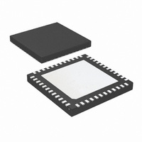
LMK02000ISQ/NOPB National Semiconductor, LMK02000ISQ/NOPB Datasheet - Page 9

LMK02000ISQ/NOPB
Manufacturer Part Number
LMK02000ISQ/NOPB
Description
IC CLOCK CONDITIONER PREC 48-LLP
Manufacturer
National Semiconductor
Type
Clock Conditionerr
Datasheet
1.LMK02000ISQNOPB.pdf
(20 pages)
Specifications of LMK02000ISQ/NOPB
Pll
Yes
Input
Clock
Output
LVDS, LVPECL
Number Of Circuits
1
Ratio - Input:output
2:8
Differential - Input:output
Yes/Yes
Frequency - Max
800MHz
Divider/multiplier
Yes/No
Voltage - Supply
3.15 V ~ 3.45 V
Operating Temperature
-40°C ~ 85°C
Mounting Type
Surface Mount
Package / Case
48-LLP
Frequency-max
800MHz
For Use With
LMK02000EVAL-1 - BOARD EVAL WITH 245.76 VCXOLMK02000EVAL2 - BOARD EVALUATION FOR LMK02000
Lead Free Status / RoHS Status
Lead free / RoHS Compliant
Other names
LMK02000ISQ
LMK02000ISQTR
LMK02000ISQTR
Available stocks
Company
Part Number
Manufacturer
Quantity
Price
Company:
Part Number:
LMK02000ISQ/NOPB
Manufacturer:
Intersil
Quantity:
106
1.0 Functional Description
The LMK02000 precision clock conditioner combines the
functions of jitter cleaning/reconditioning, multiplication, and
distribution of a reference clock. The device integrates a high
performance Integer-N Phase Locked Loop (PLL), three
LVDS, and five LVPECL clock output distribution blocks.
Each clock distribution block includes a programmable di-
vider, a phase synchronization circuit, a programmable delay,
a clock output mux, and an LVDS or LVPECL output buffer.
This allows multiple integer-related and phase-adjusted
copies of the reference to be distributed to eight system com-
ponents.
The clock conditioner comes in a 48-pin LLP package and is
footprint compatible with other clocking devices in the same
family.
1.1 BIAS PIN
To properly use the device, bypass Bias (pin 36) with a low
leakage 1 µF capacitor connected to Vcc. This is important
for low noise performance.
1.2 LDO BYPASS
To properly use the device, bypass LDObyp1 (pin 9) with a
10 µF capacitor and LDObyp2 (pin 10) with a 0.1 µF capacitor.
1.3 OSCILLATOR INPUT PORT (OSCin, OSCin*)
The purpose of OSCin is to provide the PLL with a reference
signal. The OSCin port must be AC coupled, refer to the Sys-
tem Level Diagram in the Application Information section. The
OSCin port may be driven single endedly by AC grounding
OSCin* with a 0.1 µF capacitor.
1.4 FREQUENCY INPUT PORT (Fin, Fin*)
The purpose of Fin is to provide the PLL with a feedback sig-
nal from an external oscillator. The Fin port may be driven
single endedly by AC grounding Fin*.
1.5 CLKout DELAYS
Each individual clock output includes a delay adjustment.
Clock output delay registers (CLKoutX_DLY) support a 150
ps step size and range from 0 to 2250 ps of total delay.
1.6 LVDS/LVPECL OUTPUTS
Each LVDS or LVPECL output may be disabled individually
by programming the CLKoutX_EN bits. All the outputs may
be disabled simultaneously by pulling the GOE pin low or
programming EN_CLKout_Global to 0.
1.7 GLOBAL CLOCK OUTPUT SYNCHRONIZATION
The SYNC* pin synchronizes the clock outputs. When the
SYNC* pin is held in a logic low state, the divided outputs are
also held in a logic low state. When the SYNC* pin goes high,
the divided clock outputs are activated and will transition to a
high state simultaneously. Clocks in the bypassed state are
not affected by SYNC* and are always synchronized with the
divided outputs.
The SYNC* pin must be held low for greater than one clock
cycle of the Frequency Input port, also known as the distribu-
tion path. Once this low event has been registered, the out-
puts will not reflect the low state for four more cycles. Similarly
once the SYNC* pin becomes high, the outputs will not si-
multaneously transition high until four more distribution path
clock cycles have passed. See the timing diagram below for
further detail. In the timing diagram below the clocks are pro-
9
grammed as CLKout0_MUX = Bypassed, CLKout1_MUX =
Divided, CLKout1_DIV = 2, CLKout2_MUX = Divided, and
CLKout2_DIV = 4.
SYNC* Timing Diagram
The SYNC* pin provides an internal pull-up resistor as shown
on the functional block diagram. If the SYNC* pin is not ter-
minated externally the clock outputs will operate normally. If
the SYNC* function is not used, clock output synchronization
is not guaranteed.
1.8 CLKout OUTPUT STATES
Each clock output may be individually enabled with the
CLKoutX_EN bits. Each individual output enable control bit is
gated with the Global Output Enable input pin (GOE) and the
Global Output Enable bit (EN_CLKout_Global).
All clock outputs can be disabled simultaneously if the GOE
pin is pulled low by an external signal or EN_CLKout_Global
is set to 0.
When an LVDS output is in the Off state, the outputs are at a
voltage of approximately 1.5 volts. When an LVPECL output
is in the Off state, the outputs are at a voltage of approximately
1 volt.
1.9 GLOBAL OUTPUT ENABLE AND LOCK DETECT
The GOE pin provides an internal pull-up resistor. If it is not
terminated externally, the clock output states are determined
by the Clock Output Enable bits (CLKoutX_EN) and the
EN_CLKout_Global bit.
By programming the PLL_MUX register to Digital Lock Detect
Active High (See 2.5.2), the Lock Detect (LD) pin can be con-
nected to the GOE pin in which case all outputs are set low
automatically if the synthesizer is not locked.
1.10 POWER ON RESET
When supply voltage to the device increases monotonically
from ground to Vcc, the power on reset circuit sets all registers
to their default values, see 2.3.1 for more information on de-
fault register values. Voltage should be applied to all Vcc pins
simultaneously.
Don't care
CLKoutX
_EN bit
1
0
1
EN_CLKout
_Global bit
Don't care
1
0
1
Don't care
Don't care
High / No
GOE pin
Connect
Low
Output State
www.national.com
Clock X
Enabled
Low
Off
Off
20216504


