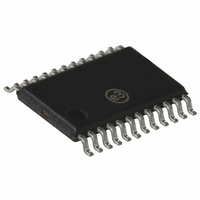
SI4112-D-GT Silicon Laboratories Inc, SI4112-D-GT Datasheet - Page 8

SI4112-D-GT
Manufacturer Part Number
SI4112-D-GT
Description
IC SYNTHESIZER IF ONLY 24TSSOP
Manufacturer
Silicon Laboratories Inc
Type
Frequency Synthesizerr
Datasheet
1.SI4112-D-GT.pdf
(36 pages)
Specifications of SI4112-D-GT
Number Of Circuits
1
Package / Case
24-TSSOP
Pll
Yes
Input
Clock
Output
Clock
Ratio - Input:output
1:2
Differential - Input:output
No/No
Frequency - Max
1GHz
Divider/multiplier
Yes/No
Voltage - Supply
2.7 V ~ 3.6 V
Operating Temperature
-40°C ~ 85°C
Mounting Type
Surface Mount
Frequency-max
1GHz
Maximum Input Frequency
62.5 MHz to 1000 MHz
Minimum Input Frequency
2 MHz
Supply Voltage (max)
3.6 V
Supply Voltage (min)
2.7 V
Maximum Operating Temperature
+ 85 C
Minimum Operating Temperature
- 40 C
Mounting Style
SMD/SMT
Operating Supply Voltage
2.7 V to 3.6 V
Lead Free Status / RoHS Status
Lead free / RoHS Compliant
Lead Free Status / RoHS Status
Lead free / RoHS Compliant, Lead free / RoHS Compliant
Other names
336-1171
Table 5. RF and IF Synthesizer Characteristics
(V
Si4133
8
Parameter
XIN Input Frequency
Reference Amplifier Sensitivity
Phase Detector Update Frequency
RF1 VCO Center Frequency Range
RF1 VCO Tuning Range
RF2 VCO Center Frequency Range
RF Tuning Range from f
IF VCO Center Frequency Range
IFOUT Tuning Range
IFOUT Tuning Range from f
RF1 VCO Pushing
RF2 VCO Pushing
IF VCO Pushing
RF1 VCO Pulling
RF2 VCO Pulling
IF VCO Pulling
RF1 Phase Noise
RF1 Integrated Phase Error
RF2 Phase Noise
RF2 Integrated Phase Error
IF Phase Noise
IF Integrated Phase Error
Notes:
DD
1. f
2. Extended frequency operation only. V
3. From powerup request (PWDN or SEN during a write of 1 to bits PDIB and PDRB in Register 2) to RF and IF
4. From powerdown request (PWDN, or SENduring a write of 0 to bits PDIB and PDRB in Register 2) to supply current
= 2.7 to 3.6 V, T
RFLB pins. See Application Note 41 for more details on the Si4133 extended frequency operation.
synthesizers ready (settled to within 0.1 ppm frequency error).
equal to I
= 200 kHz, RF1 = 1.6 GHz, RF2 = 1.2 GHz, IFOUT = 550 MHz, LPWR = 0, for all parameters unless otherwise noted.
1
PWDN
A
.
= –40 to 85 °C)
CEN
2
CEN
DD
Symbol
3.0 V, QFN only, VCO Tuning Range fixed by directly shorting the RFLA and
V
f
f
f
f
CEN
CEN
CEN
REF
f
REF
Rev. 1.61
Extended frequency
100 Hz to 100 kHz
phases, open loop
Note: L
Note: L
10 Hz to 100 kHz
10 Hz to 100 kHz
VSWR = 2:1, all
Test Condition
100 kHz offset
1 MHz offset
1 MHz offset
with IFDIV
Open loop
f
operation
= f
EXT
EXT
REF
/R
±10%
±10%
0.010
1850
62.5
Min
947
789
526
0.5
–5
–5
—
—
—
—
—
—
—
—
—
—
—
—
2
–132
–134
–117
Typ
500
400
300
400
300
100
0.9
0.7
0.4
—
—
—
—
—
—
—
—
—
—
+0.3 V
1720
2050
1429
1000
Max
V
952
1.0
26
—
—
—
—
—
—
—
—
—
—
—
—
5
5
DD
degrees
degrees
degrees
dBc/Hz
dBc/Hz
dBc/Hz
kHz
kHz
kHz
kHz/V
kHz/V
kHz/V
MHz
MHz
MHz
MHz
MHz
MHz
MHz
Unit
V
rms
rms
rms
%
%
PP
PP
PP
PP


