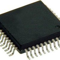
CY7B9945V-5AXC Cypress Semiconductor Corp, CY7B9945V-5AXC Datasheet - Page 6

CY7B9945V-5AXC
Manufacturer Part Number
CY7B9945V-5AXC
Description
IC CLK BUFF 11OUT 200MHZ 52LQFP
Manufacturer
Cypress Semiconductor Corp
Type
Clock Buffer, Fanout Distributionr
Series
RoboClock™r
Datasheet
1.CY7B9945V-5AXC.pdf
(13 pages)
Specifications of CY7B9945V-5AXC
Number Of Circuits
1
Package / Case
52-LQFP
Pll
Yes
Input
LVPECL, LVTTL
Output
LVTTL
Ratio - Input:output
4:10
Differential - Input:output
Yes/No
Frequency - Max
200MHz
Divider/multiplier
Yes/Yes
Voltage - Supply
2.97 V ~ 3.63 V
Operating Temperature
0°C ~ 70°C
Mounting Type
Surface Mount
Frequency-max
200MHz
Maximum Input Frequency
200 MHz
Minimum Input Frequency
24 MHz
Output Frequency Range
24 MHz to 200 MHz
Supply Voltage (max)
3.63 V
Supply Voltage (min)
2.97 V
Maximum Operating Temperature
+ 70 C
Minimum Operating Temperature
0 C
Mounting Style
SMD/SMT
Operating Supply Voltage
3.3 V
Lead Free Status / RoHS Status
Lead free / RoHS Compliant
Available stocks
Company
Part Number
Manufacturer
Quantity
Price
Company:
Part Number:
CY7B9945V-5AXC
Manufacturer:
Cypress Semiconductor Corp
Quantity:
10 000
Company:
Part Number:
CY7B9945V-5AXCT
Manufacturer:
Cypress Semiconductor Corp
Quantity:
10 000
Document Number: 38-07336 Rev. *H
Output Disable Description
The output of each output bank can be independently put into a
HOLD OFF or high impedance state. The combination of the
MODE and DIS[1:2] inputs determines the clock outputs’ state
for each bank. When the DIS[1:2] is LOW, the outputs of the
corresponding banks are enabled. When DIS[1:2] is HIGH, the
outputs for that bank are disabled to a high impedance (HI-Z) or
HOLD OFF state.
The HOLD OFF state is a power saving feature. An output bank
is disabled to the HOLD OFF state in a maximum of six output
clock cycles from the time the disable input is HIGH. When
disabled to the HOLD OFF state, outputs are driven to a logic
LOW state on their falling edges. This makes certain that the
Notes
1. FB connected to an output selected for “Zero” skew (i.e., FBF0 = MID or XF[1:0] = MID).
2. The level set on FS is determined by the “nominal” operating frequency (f
3. BK1Q denotes following the skew setting of indicated Bank1 outputs.
4. These inputs are normally wired to V
5. This is for non-three level inputs.
is operating in the undivided mode. The REF and FB are at f
unconnected inputs at V
all data sheet limits are achieved.
Table 5
CC
/2. If these inputs are switched, the function and timing of the outputs may glitch and the PLL may require an additional t
defines the disabled outputs functions.
CC
, GND, or left unconnected (actual threshold voltages vary as a percentage of V
PRELIMINARY
NOM
when the output connected to FB is undivided.
NOM
) of the V
output clocks are stopped without a glitch. When a bank of
outputs is disabled to HI-Z state, the respective bank of outputs
go High-Z immediately.
Table 5. DIS[1:2] Functionality
HIGH/LOW
CO
MODE
and Phase Generator. f
HIGH
LOW
MID
DIS[1:2]
HIGH
HIGH
LOW
NOM
X
always appears on an output when the output
CC
). Internal termination resistors hold the
1Q[0:3], 2Q[0:5]
FACTORY TEST
HOLD-OFF
RoboClock
ENABLED
CY7B9945V
HI-Z
LOCK
Page 6 of 13
time before
[+] Feedback


