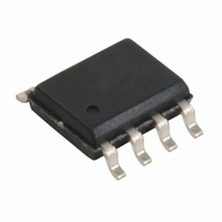
CY2302SXC-1 Cypress Semiconductor Corp, CY2302SXC-1 Datasheet - Page 3

CY2302SXC-1
Manufacturer Part Number
CY2302SXC-1
Description
IC CLK FREQ MULTI/ZDB 2OUT 8SOIC
Manufacturer
Cypress Semiconductor Corp
Type
Fanout Distribution, Frequency Multiplier, Zero Delay Bufferr
Datasheet
1.CY2302SXI-1.pdf
(9 pages)
Specifications of CY2302SXC-1
Number Of Circuits
1
Package / Case
8-SOIC (3.9mm Width)
Pll
Yes
Input
LVCMOS, LVTTL
Output
LVCMOS
Ratio - Input:output
1:2
Differential - Input:output
No/No
Frequency - Max
133MHz
Divider/multiplier
Yes/Yes
Voltage - Supply
3.3V, 5V
Operating Temperature
0°C ~ 70°C
Mounting Type
Surface Mount
Frequency-max
133MHz
Maximum Input Frequency
133 MHz
Minimum Input Frequency
5 MHz
Output Frequency Range
10 MHz to 133 MHz
Supply Voltage (max)
5.5 V
Supply Voltage (min)
3.135 V
Maximum Operating Temperature
+ 70 C
Minimum Operating Temperature
0 C
Mounting Style
SMD/SMT
Operating Supply Voltage
3.3 V, 5 V
Clock Ic Type
Clock Buffer
Frequency
133MHz
No. Of Outputs
2
No. Of Multipliers / Dividers
1
Supply Current
37mA
Supply Voltage Range
3.135V To 3.465V, 4.5V To 5.5V
Digital Ic Case Style
SOIC
Rohs Compliant
Yes
Number Of Elements
1
Pll Input Freq (min)
5MHz
Pll Input Freq (max)
133MHz
Operating Supply Voltage (typ)
3.3/5V
Operating Temp Range
0C to 70C
Package Type
SOIC
Operating Supply Voltage (min)
3.135V
Operating Supply Voltage (max)
5.5V
Operating Temperature Classification
Commercial
Pin Count
8
Lead Free Status / RoHS Status
Lead free / RoHS Compliant
Lead Free Status / RoHS Status
Lead free / RoHS Compliant, Lead free / RoHS Compliant
Other names
428-2187-5
CY2302SXC-1
CY2302SXC-1
Available stocks
Company
Part Number
Manufacturer
Quantity
Price
Company:
Part Number:
CY2302SXC-1
Manufacturer:
CYPRESS
Quantity:
25
Part Number:
CY2302SXC-1
Manufacturer:
CYPRESS/赛普拉斯
Quantity:
20 000
Overview
The CY2302 is a two-output zero delay buffer and frequency multiplier. It provides an external feedback path allowing maximum
flexibility when implementing the Zero Delay feature. This is explained further in the sections of this datasheet titled,
Zero Delay on page
The CY2302 is a pin-compatible upgrade of the Cypress W42C70-01. The CY2302 addresses some application dependent problems
experienced by users of the older device.
How to Implement Zero Delay
Typically, Zero Delay Buffers (ZDBs) are used because a
designer wants to provide multiple copies of a clock signal in
phase with each other. The whole concept behind ZDBs is that
the signals at the destination chips are all going HIGH at the
same time as the input to the ZDB. In order to achieve this, layout
must compensate for trace length between the ZDB and the
target devices. The method of compensation is described as
follows.
External feedback is the trait that allows for this compensation.
The PLL on the ZDB causes the feedback signal to be in phase
with the reference signal. When laying out the board, match the
trace lengths between the output being used for feedback and
the FBIN input to the PLL.
If it is desirable to either add a little delay, or slightly precede the
input signal, this may also be implemented by either making the
trace to the FBIN pin a little shorter or a little longer than the
traces to the devices being clocked.
Inserting Other Devices in Feedback Path
Another nice feature available due to the external feedback is the
ability to synchronize signals to the signal coming from some
other device. This implementation can be applied to any device
(ASIC, multiple output clock buffer/driver, etc.) that is put into the
feedback path.
Referring to
the destination of the clock signal(s) (A) are equal in length to the
Document #: 38-07154 Rev. *E
Figure
2, if the traces between the ASIC/Buffer and
3, and
FBIN
FS0
IN
Inserting Other Devices in Feedback Path on page
GND
G
Figure 2. Schematic/Suggested Layout
1
2
3
4
G
10 µ F
C
A
0.01 µ F
Ferrite
Bead
C8
trace between the buffer and the FBIN pin, the signals at the
destination(s) device is driven HIGH at the same time when the
Reference clock provided to the ZDB goes HIGH. Synchronizing
the other outputs of the ZDB to the outputs from the ASIC/Buffer
is more complex however, as any propagation delay from the
ZDB output to the ASIC/Buffer output must be accounted for.
Figure 3. Six Output Buffer in the Feedback Path
Phase Alignment
In cases where OUT1 (i.e., the higher frequency output) is
connected to FBIN input pin the output OUT2 rising edges may
be either 0 or 180 phase aligned to the IN input waveform (as
set randomly when the input and/or power is supplied). If OUT2
is desired to be rising-edge aligned to the IN input’s rising edge,
then connect the OUT2 (i.e., the lowest frequency output) to the
FBIN pin. This set-up provides a consistent input-output phase
relationship.
6
5
8
7
Reference
Feedback
V+
Signal
Input
G
Power Supply Connection
OUT 2
V
OUT 1
DD
3.
Zero
Delay
Buffer
FS1
22
22
C9 = 0.1 µ F
G
OUTPUT 2
OUTPUT 1
Buffer
ASIC/
How to Implement
CY2302
Page 3 of 9
A
[+] Feedback


