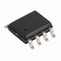
CY2302SXC-1 Cypress Semiconductor Corp, CY2302SXC-1 Datasheet - Page 2

CY2302SXC-1
Manufacturer Part Number
CY2302SXC-1
Description
IC CLK FREQ MULTI/ZDB 2OUT 8SOIC
Manufacturer
Cypress Semiconductor Corp
Type
Fanout Distribution, Frequency Multiplier, Zero Delay Bufferr
Datasheet
1.CY2302SXI-1.pdf
(9 pages)
Specifications of CY2302SXC-1
Number Of Circuits
1
Package / Case
8-SOIC (3.9mm Width)
Pll
Yes
Input
LVCMOS, LVTTL
Output
LVCMOS
Ratio - Input:output
1:2
Differential - Input:output
No/No
Frequency - Max
133MHz
Divider/multiplier
Yes/Yes
Voltage - Supply
3.3V, 5V
Operating Temperature
0°C ~ 70°C
Mounting Type
Surface Mount
Frequency-max
133MHz
Maximum Input Frequency
133 MHz
Minimum Input Frequency
5 MHz
Output Frequency Range
10 MHz to 133 MHz
Supply Voltage (max)
5.5 V
Supply Voltage (min)
3.135 V
Maximum Operating Temperature
+ 70 C
Minimum Operating Temperature
0 C
Mounting Style
SMD/SMT
Operating Supply Voltage
3.3 V, 5 V
Clock Ic Type
Clock Buffer
Frequency
133MHz
No. Of Outputs
2
No. Of Multipliers / Dividers
1
Supply Current
37mA
Supply Voltage Range
3.135V To 3.465V, 4.5V To 5.5V
Digital Ic Case Style
SOIC
Rohs Compliant
Yes
Number Of Elements
1
Pll Input Freq (min)
5MHz
Pll Input Freq (max)
133MHz
Operating Supply Voltage (typ)
3.3/5V
Operating Temp Range
0C to 70C
Package Type
SOIC
Operating Supply Voltage (min)
3.135V
Operating Supply Voltage (max)
5.5V
Operating Temperature Classification
Commercial
Pin Count
8
Lead Free Status / RoHS Status
Lead free / RoHS Compliant
Lead Free Status / RoHS Status
Lead free / RoHS Compliant, Lead free / RoHS Compliant
Other names
428-2187-5
CY2302SXC-1
CY2302SXC-1
Available stocks
Company
Part Number
Manufacturer
Quantity
Price
Company:
Part Number:
CY2302SXC-1
Manufacturer:
CYPRESS
Quantity:
25
Part Number:
CY2302SXC-1
Manufacturer:
CYPRESS/赛普拉斯
Quantity:
20 000
Pinouts
Table 2. Pin Definition
Document #: 38-07154 Rev. *E
Pin Name
OUT1
OUT2
FS0:1
FBIN
GND
VDD
IN
Pin No
4, 5
2
1
6
8
7
3
Type
Pin
O
O
P
P
I
I
I
Reference Input: The output signals are synchronized to this signal.
Feedback Input: This input must be fed by one of the outputs (OUT1 or OUT2) to ensure
Function Select Inputs: Tie to V
Figure 1. Pin Configuration – 8-Pin SOIC Package
proper functionality. If the trace between FBIN and the output pin being used for feedback is
equal in length to the traces between the outputs and the signal destinations, then the signals
received at the destinations are synchronized to the REF signal input (IN).
Output 1: The frequency of the signal provided by this pin is determined by the feedback
signal connected to FBIN, and the FS0:1 inputs (see
Output 2: The frequency of the signal provided by this pin is one-half of the frequency of
OUT1. See
Power Connections: Connect to 3.3V or 5V. This pin should be bypassed with a 0.1-F
decoupling capacitor. Use ferrite beads to help reduce noise for optimal jitter performance.
Ground Connection: Connect all grounds to the common system ground plane.
FBIN
GND
FS0
IN
Table
1.
1
2
3
4
DD
8
7
6
5
(HIGH, 1) or GND (LOW, 0) as desired per
Pin Description
OUT2
VDD
OUT1
FS1
Table
1).
Table
CY2302
Page 2 of 9
1.
[+] Feedback


