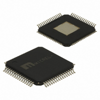
SY89828LHI Micrel Inc, SY89828LHI Datasheet - Page 3

SY89828LHI
Manufacturer Part Number
SY89828LHI
Description
IC BUFFER DUAL 1:10 IVDS 64-TQFP
Manufacturer
Micrel Inc
Series
Precision Edge®r
Type
Fanout Buffer (Distribution), Multiplexer , Translatorr
Datasheet
1.SY89828LHY.pdf
(13 pages)
Specifications of SY89828LHI
Number Of Circuits
2
Ratio - Input:output
2:10
Differential - Input:output
Yes/Yes
Input
LVDS, PECL
Output
LVDS
Frequency - Max
1GHz
Voltage - Supply
3 V ~ 3.6 V
Operating Temperature
-40°C ~ 85°C
Mounting Type
Surface Mount
Package / Case
64-TQFP Exposed Pad, 64-eTQFP, 64-HTQFP, 64-VQFP
Frequency-max
1GHz
Clock Ic Type
Clock Divider / Fan-out Buffer
Frequency
1GHz
No. Of Outputs
10
Ic Output Type
LVDS
Supply Current
45mA
Supply Voltage Range
3V To 3.6V
Digital Ic Case Style
TQFP
No. Of Pins
64
Lead Free Status / RoHS Status
Contains lead / RoHS non-compliant
Available stocks
Company
Part Number
Manufacturer
Quantity
Price
MicreL, Inc.
M9999-012208
hbwhelp@micrel.com or (408) 955-1690
63, 61, 59, 57, 55
53, 51, 47, 45, 43
62, 60, 58, 56, 54
52, 50, 46, 44, 42
39, 37, 35, 31, 29
27, 25, 23, 21, 19
PIN DESCRIPTIONS
Pin Number
17, 32, 40,
41, 49, 64
12, 13
33, 48
5, 6
2, 3
8, 9
14
16
11
15
10
7
1
4
/LVPECL_CLKA
/LVPECL_CLKB
LVPECL_CLKA
LVPECL_CLKB
/LVDS_CLKA
/LVDS_CLKB
LVDS_CLKA
LVDS_CLKB
CLK_SEL1
CLK_SEL2
Q10 – Q19
Pin Name
/Q0 – /Q9
Q0 – Q9
GNDO
VCCO
GNDI
SEL1
SEL2
VCCI
OE1
OE2
Output
Output
Output
Power
Power
Power
Power
Input
Input
Input
Input
Input
Input
Input
Input
Input
Input
I/O
LVPECL
LVPECL
LVTTL/
LVTTL/
LVTTL/
LVTTL/
LVTTL/
LVTTL/
CMOS
CMOS
CMOS
CMOS
CMOS
CMOS
LVDS
LVDS
LVDS
LVDS
LVDS
Type
See Fig. 2
See Fig. 2
See Fig. 1
See Fig. 1
pull-down
pull-down
Internal
Pull-up
Pull-up
Pull-up
Pull-up
Pull-up
Pull-up
Pull-up
Pull-up
3.5kΩ
3.5kΩ
75kΩ
75kΩ
11kΩ
11kΩ
11kΩ
11kΩ
11kΩ
11kΩ
P/U
3
Pin Function
Differential clock input selected by CLK_SEL1, SEL1 and
SEL2. Can be left floating if not selected. Floating input, if
selected produces an indeterminate output. Has internal
100Ω termination.
Differential clock input selected by CLK_SEL1, SEL1 and
SEL2. Can be left floating if not selected. Floating input, if
selected produces an indeterminate output. Has internal
100Ω termination.
Differential clock input selected by CLK_SEL1, SEL1
and SEL2. Can be left floating. Floating input, if selected
produces a LOW at output. Requires external termination.
Differential clock input selected by CLK_SEL2, SEL1
and SEL2. Requires external termination.
Selects LVDS_CLKA input when LOW and
LVPECL_CLKA input when HIGH.
Selects LVDS_CLKB input when LOW and
LVPECL_CLKB input when HIGH.
Selects input source CLKA when LOW and CLKB
when HIGH for outputs Q0 – Q9 and /Q0 – /Q9.
Selects input source CLKA when LOW and CLKB
when HIGH for outputs Q10 – Q19 and /Q10 – /Q19.
Enable input synchronized internally to prevent output
glitches or runt pulses.
Enable input synchronized internally to prevent output
glitches or runt pulses.
Core VCC connected to 3.3V supply. Not connected to
VCCO internally. Connected to VCCO on PCB.
Bypass with 0.1µF in parallel with 0.01µF low ESR
capacitors as close to VCC pins as possible.
Output buffer VCC connected to 3.3V suppy. Not connected
to VCCI internally. Connected to VCCI on PCB.
Bypass with 0.1µF in parallel with 0.01µF low ESR
capacitors as close to VCC pins as possible.
Core ground not connected to GNDO internally.
To be connected to GNDO on PCB.
Output buffer ground not connected to GNDI internally.
To be connected to GNDI on PCB.
Differential clock outputs from CLKA when SEL1 = LOW
and from CLKB when SEL1 = HIGH. Q outputs are static
when OE1 = LOW. Unused output pair must be terminated
with 100Ω to maintain low jitter and skew.
Differential clock outputs (complement) from CLKA when
SEL1 = LOW and from CLKB when SEL1 = HIGH. /Q
outputs are static HIGH when OE1 = LOW. Unused output
pairs must be externally terminated with 100Ω to maintain
low jitter and skew.
Differential outputs from CLKA when SEL2 = LOW and
from CLKB when SEL2 = HIGH. Q outputs are static LOW
when OE2 = LOW. Unused output pairs must be externally
terminated with 100Ω to maintain low jitter and skew.
Precision Edge
SY89828L
®


