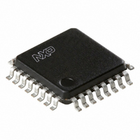
PCK9456BD,151 NXP Semiconductors, PCK9456BD,151 Datasheet - Page 9

PCK9456BD,151
Manufacturer Part Number
PCK9456BD,151
Description
IC FANOUT BUFFER LVCMOS 32LQFP
Manufacturer
NXP Semiconductors
Type
Fanout Buffer (Distribution), Divider, Multiplexerr
Datasheet
1.PCK9456BD151.pdf
(18 pages)
Specifications of PCK9456BD,151
Number Of Circuits
1
Ratio - Input:output
1:10
Differential - Input:output
Yes/No
Input
LVPECL
Output
LVCMOS
Frequency - Max
250MHz
Voltage - Supply
2.375 V ~ 3.465 V
Operating Temperature
-40°C ~ 85°C
Mounting Type
Surface Mount
Package / Case
32-LQFP
Frequency-max
250MHz
Lead Free Status / RoHS Status
Lead free / RoHS Compliant
Other names
568-3644-5
935280285151
PCK9456BD-S
935280285151
PCK9456BD-S
Available stocks
Company
Part Number
Manufacturer
Quantity
Price
Company:
Part Number:
PCK9456BD,151
Manufacturer:
NXP Semiconductors
Quantity:
10 000
Philips Semiconductors
Table 12.
T
[1]
[2]
[3]
PCK9456_1
Product data sheet
Symbol
t
t
t
t
t
sk(o)
sk(pr)
sk(p)
PLH
PHL
amb
Fig 3. Output transition time test reference
Fig 5. Propagation delay (t
o
Dynamic (AC) characteristics apply for parallel output termination of 50
For all other dynamic (AC) specifications, refer to 2.5 V or 3.3 V tables according to the supply voltage of the output bank.
Output pulse skew is the absolute difference of the propagation delay times: t
= 40 C to +85 C; V
(1) 2.4 V (V
(2) 0.55 V (V
1.8 V (V
0.6 V (V
PCLK
PCLK
Qn
Dynamic characteristics
Parameter
output skew time
process skew time
pulse skew time
LOW-to-HIGH propagation delay
HIGH-to-LOW propagation delay
output duty cycle
CC
CC
CC
CC
= 3.3 V)
= 2.5 V)
= 2.5 V)
V
= 3.3 V)
t
f
i(p-p)
t
PLH
CC
= 3.3 V
PD
t
r
) test reference
t
PHL
002aab292
5 %; V
(2)
(1)
002aab875
CC(bankA)
V
0.5V
GND
V
CC
ICR
Conditions
output-to-output
part-to-part
output
PCLK to any Q
PCLK to any Q
CC
ref
Rev. 01 — 31 July 2006
within one bank
any output bank,
same output divider
any output,
any output divider
= 50 %
= V
CC(bankB)
Fig 4. Output duty cycle (
Fig 6. Output-to-output skew (t
= V
to V
CC(bankC)
2.5 V and 3.3 V LVCMOS clock fan-out buffer
The time from the PLL controlled edge to the
non-controlled edge, divided by the time between
PLL controlled edges, expressed as a percentage.
The pin-to-pin skew is defined as the worst-case
difference in propagation delay between any similar
delay path within a single device.
PLH
T
.
o
= (t
[3]
t
PHL
p
= 2.5 V
t
Min
-
-
-
-
-
see
see
45
sk(o)
.
T
o
t
p
Table 10
Table 10
100 %)
© Koninklijke Philips Electronics N.V. 2006. All rights reserved.
T
5 % or 3.3 V
o
Typ
-
-
-
-
-
50
o
)
sk(o)
)
PCK9456
002aab291
t
sk(o)
Max
150
250
350
2.5
250
55
5 %
V
0.5V
GND
CC
002aab289
[1][2]
CC
V
0.5V
GND
V
0.5V
GND
CC
CC
CC
CC
Unit
ns
%
ps
ps
ps
ps
9 of 18


