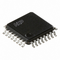
PCK9446BD,151 NXP Semiconductors, PCK9446BD,151 Datasheet - Page 4

PCK9446BD,151
Manufacturer Part Number
PCK9446BD,151
Description
IC FANOUT BUFFER LVCMOS 32LQFP
Manufacturer
NXP Semiconductors
Type
Fanout Buffer (Distribution), Divider, Multiplexerr
Datasheet
1.PCK9446BD151.pdf
(17 pages)
Specifications of PCK9446BD,151
Number Of Circuits
1
Ratio - Input:output
2:10
Differential - Input:output
No/No
Input
LVCMOS
Output
LVCMOS
Frequency - Max
250MHz
Voltage - Supply
2.375 V ~ 3.465 V
Operating Temperature
-40°C ~ 85°C
Mounting Type
Surface Mount
Package / Case
32-LQFP
Frequency-max
250MHz
Lead Free Status / RoHS Status
Lead free / RoHS Compliant
Other names
568-3643-5
935280839151
PCK9446BD-S
935280839151
PCK9446BD-S
Available stocks
Company
Part Number
Manufacturer
Quantity
Price
Company:
Part Number:
PCK9446BD,151
Manufacturer:
NXP Semiconductors
Quantity:
10 000
Philips Semiconductors
6. Functional description
PCK9446_1
Product data sheet
6.1 Function table
6.2 Supply configurations
Refer to
Table 3.
Table 4.
[1]
[2]
[3]
[4]
Control
CLK_SEL 0
FSELA
FSELB
FSELC
MR/OE
Supply voltage
configuration
3.3 V
mixed voltage supply
2.5 V
V
threshold and levels.
V
bank A output levels.
V
bank B output levels. V
V
bank C output levels.
CC
CC(bankA)
CC(bankB)
CC(bankC)
is the positive power supply of the device core and input circuitry. V
Figure 1 “Logic diagram of
Function table (controls)
Supported single and dual supply configurations
Default
0
0
0
0
is the positive power supply of the bank A outputs (VCCA pins). V
is the positive power supply of the bank B outputs (VCCB pins). V
is the positive power supply of the bank C outputs (VCCC pins). V
Value
0
CLK0
frequency on bank A outputs = f
frequency on bank B outputs = f
frequency on bank C outputs = f
outputs enabled
CCB
V
3.3 V
3.3 V
2.5 V
Rev. 01 — 10 April 2006
CC
is internally connected to V
[1]
V
3.3 V
3.3 V or 2.5 V
2.5 V
PCK9446”.
CC(bankA)
2.5 V and 3.3 V LVCMOS clock fan-out buffer
[2]
CC
.
ref
ref
ref
V
3.3 V
3.3 V
2.5 V
CC(bankB)
1
CLK1
frequency on bank A outputs = f
frequency on bank B outputs = f
frequency on bank C outputs = f
internal reset outputs disabled (3-state)
© Koninklijke Philips Electronics N.V. 2006. All rights reserved.
[3]
CC
voltage defines the input
V
3.3 V
3.3 V or 2.5 V
2.5 V
CC(bankA)
CC(bankB)
CC(bankC)
CC(bankC)
PCK9446
voltage defines
voltage defines
voltage defines
[4]
GND
0 V
0 V
0 V
ref
ref
ref
4 of 17
2
2
2


