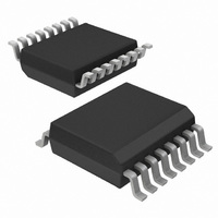
PCK2001RDB,118 NXP Semiconductors, PCK2001RDB,118 Datasheet - Page 8

PCK2001RDB,118
Manufacturer Part Number
PCK2001RDB,118
Description
IC 1:6 CLOCK BUFFER 16SSOP
Manufacturer
NXP Semiconductors
Type
Fanout Buffer (Distribution)r
Datasheet
1.PCK2001RDB118.pdf
(12 pages)
Specifications of PCK2001RDB,118
Number Of Circuits
1
Ratio - Input:output
1:6
Differential - Input:output
No/No
Input
LVTTL
Output
LVTTL
Frequency - Max
533MHz
Voltage - Supply
3.135 V ~ 3.465 V
Operating Temperature
0°C ~ 70°C
Mounting Type
Surface Mount
Package / Case
16-SSOP
Frequency-max
533MHz
Lead Free Status / RoHS Status
Lead free / RoHS Compliant
Other names
935268179118
PCK2001RDB-T
PCK2001RDB-T
PCK2001RDB-T
PCK2001RDB-T
Philips Semiconductors
SERIAL CONFIGURATION MAP
The serial bits will be read by the clock buffer in the following order:
All unused register bits (Reserved and N/A) should be desined as “Don’t Care”. It is expected that the controller will force all of these bits to a
“0” level.
All register bits labeled “Initialize to 0” must be written to zero during intialization. Failure to do so may result in a higher than normal operating
current. The controller will read back the last written value.
Byte 0: Active/inactive register
1 = enable; 0 = disable
NOTE:
1. Inactive means outputs are held LOW and are disabled from switching. These outputs are designed to be configured at power-on and are
Byte 1: Active/inactive register
1 = enable; 0 = disable
NOTE:
1. Inactive means outputs are held LOW and are disabled from switching. These outputs are designed to be configured at power-on and are
Byte 2: Active/inactive register
NOTE:
1. Inactive means outputs are held LOW and are disabled from switching. These outputs are designed to be configured at power-on and are
2002 Dec 13
533 MHz I
Byte 0 - Bits 7, 6, 5, 4, 3, 2, 1, 0
Byte 1 - Bits 7, 6, 5, 4, 3, 2, 1, 0
Byte 2 - Bits 7, 6, 5, 4, 3, 2, 1, 0
not expected to be configured during the normal modes of operation.
not expected to be configured during the normal modes of operation.
not expected to be configured during the normal modes of operation.
BIT
BIT
BIT
7
6
5
4
3
2
1
0
7
6
5
4
3
2
1
0
7
6
5
4
3
2
1
0
PIN#
PIN#
PIN#
2
15
13
—
—
—
—
—
—
—
—
—
—
—
11
—
—
—
—
—
—
—
6
3
1
C 1:6 clock buffer
BUF_OUT14
BUF_OUT11
BUF_OUT17
BUF_OUT7
BUF_OUT2
BUF_OUT0
NAME
NAME
NAME
—
—
—
—
—
—
—
—
—
—
—
—
—
—
—
—
—
—
8
DESCRIPTION
DESCRIPTION
DESCRIPTION
Active/Inactive
Active/Inactive
Active/Inactive
Active/Inactive
Active/Inactive
Active/Inactive
—
—
—
—
—
—
—
—
—
—
—
—
—
—
—
—
—
—
PCK2001R
Product data


