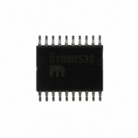
SY898533LKZ Micrel Inc, SY898533LKZ Datasheet - Page 5

SY898533LKZ
Manufacturer Part Number
SY898533LKZ
Description
IC BUFFER 1:4 LVPECL 20-TSSOP
Manufacturer
Micrel Inc
Series
Precision Edge®r
Type
Fanout Buffer (Distribution), Multiplexerr
Datasheet
1.SY898533LKZ.pdf
(11 pages)
Specifications of SY898533LKZ
Number Of Circuits
1
Ratio - Input:output
2:4
Differential - Input:output
Yes/Yes
Input
CML, HCSL, LVDS, LVHSTL, LVPECL, SSTL
Output
LVPECL
Frequency - Max
650MHz
Voltage - Supply
3.135 V ~ 3.465 V
Operating Temperature
0°C ~ 70°C
Mounting Type
Surface Mount
Package / Case
20-TSSOP
Frequency-max
650MHz
Lead Free Status / RoHS Status
Lead free / RoHS Compliant
Other names
576-3560-5
Available stocks
Company
Part Number
Manufacturer
Quantity
Price
Company:
Part Number:
SY898533LKZ
Manufacturer:
Micrel Inc
Quantity:
135
Micrel, Inc.
LVPECL DC Electrical Characteristics
V
Notes:
7. The circuit is designed to meet the DC specifications shown in the above table after thermal equilibrium has been established.
8. Maximum input voltage for PCLK and /PCLK is V
9. V
10. 50Ω to V
AC Electrical Characteristics
V
Notes:
11. High-frequency AC-parameters are guaranteed by design and characterization.
12. Output-to-Output skew is measured between two different outputs under identical transitions.
13. Part-to-Part skew is defined for two parts with identical power supply voltages at the same temperature and with no skew of the edges at the
14. Driving only one input clock.
July 2009
Symbol
I
I
V
V
V
V
V
Symbol
f
t
t
t
t
odc
CC
CC
IH
IL
MAX
PD
SKEW
JITTER
r,
PP
CMR
OH
OL
SWING
t
f
respective inputs. This parameter is defined in accordance with JEDEC Standard 65.
= 3.3V ±5%; T
IH
= 3.3V ±5%; R
is defined as the common mode voltage.
CC
Parameter
Input High Current
Input Low Current
Peak-to-Peak Input Voltage
Common Mode Input Voltage
Output High Voltage
Output Low Voltage
Peak-to-Peak Output Voltage
Swing
Parameter
Maximum Operating Frequency
Differential Propagation Delay
IN-to-Q
Output-to-Output Skew
Part-to-Part Skew
Additive Phase Jitter
Output Rise/Fall Time
Output Duty Cycle
-2V terminated outputs.
A
L
= 0°C to +70°C, unless otherwise stated.
= 50Ω to V
(13)
(10)
(10)
(14)
CC
(12)
-2V; T
/PCLK
/PCLK
PCLK
PCLK
(8, 9)
A
(11)
= 0°C to +70°C, unless otherwise stated.
CC
Condition
V
V
V
V
+ 0.3V for single ended applications.
Condition
f ≤ 650MHz
20% to 80% @ 50MHz
IN
IN
IN
IN
= V
= V
= 0V, V
= 0V, V
CC
CC
(7)
= 3.465V
= 3.465V
CC
CC
= 3.465V
= 3.465V
6
V
V
V
EE
CC
CC
-150
Min
Min
650
300
0.3
0.6
1.0
47
-5
+ 1.5
– 2.0
hbwhelp@micrel.com
- 1.4
0.06
Typ
Typ
V
V
or (408) 955-1690
CC
CC
Max
M9999-072409-C
150
700
Max
1.4
150
V
30
53
1.0
5
1
CC
– 0.9
- 1.7
SY898533L
ps
Units
MHz
Units
ns
ps
ps
ps
%
µA
µA
µA
µA
RMS
V
V
V
V
V


