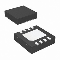
LMV112SD/NOPB National Semiconductor, LMV112SD/NOPB Datasheet - Page 2

LMV112SD/NOPB
Manufacturer Part Number
LMV112SD/NOPB
Description
IC CLOCK BUFFER DUAL 40MHZ 8-LLP
Manufacturer
National Semiconductor
Type
Fanout Buffer (Distribution)r
Datasheet
1.LMV112SDNOPB.pdf
(14 pages)
Specifications of LMV112SD/NOPB
Number Of Circuits
2
Ratio - Input:output
2:2
Differential - Input:output
No/No
Input
Clock
Output
Clock
Frequency - Max
40MHz
Voltage - Supply
2.4 V ~ 5.0 V
Operating Temperature
-40°C ~ 85°C
Mounting Type
Surface Mount
Package / Case
8-LLP
Frequency-max
40MHz
Slew Rate
110V/µs
Supply Voltage Range
2.4V To 5V
Logic Case Style
LLP
No. Of Pins
8
Operating Temperature Range
-40°C To +85°C
Msl
MSL 1 - Unlimited
Single Supply Voltage Min (+v)
2.4V
Rohs Compliant
Yes
Amplifier Case Style
LLP
For Use With
LMV112SDEVAL - BOARD EVALUATION FOR LMV112SD
Lead Free Status / RoHS Status
Lead free / RoHS Compliant
Other names
*LMV112SD
LMV112SD
LMV112SDNOPB
LMV112SDNOPBTR
LMV112SDNOPBTR
LMV112SDTR
LMV112SD
LMV112SDNOPB
LMV112SDNOPBTR
LMV112SDNOPBTR
LMV112SDTR
Available stocks
Company
Part Number
Manufacturer
Quantity
Price
Company:
Part Number:
LMV112SD/NOPB
Manufacturer:
TI
Quantity:
144
www.national.com
Frequency Domain Response
SSBW
FPBW
GFN
Distortion and Noise Performance
e
I
CT
Time Domain Response
t
t
t
OS
SR
Static DC Performance
I
PSRR
A
V
TC V
R
Miscellaneous Performance
R
C
Z
SOLATION
r
f
s
S
Symbol
n
IN
CL
OS
OUT
IN
IN
Absolute Maximum Ratings
If Military/Aerospace specified devices are required,
please contact the National Semiconductor Sales Office/
Distributors for availability and specifications.
2.7V Electrical Characteristics
Unless otherwise specified, all limits are guaranteed for T
pF, R
Supply Voltages (V
ESD Tolerance (Note 2)
Storage Temperature Range
Junction Temperature (Note 3)
OS
Human Body
Machine Model
L
= 30 kΩ, C
Small Signal Bandwidth
Full Power Bandwidth
Gain Flatness
Input-Referred Voltage Noise
Output to Input
Crosstalk Rejection
Rise Time
Fall Time
Settling Time to 0.1%
Overshoot
Slew Rate (Note 7)
Supply Current
Power Supply Rejection Ratio
Small Signal Voltage Gain
Output Offset Voltage
Temperature Coefficient Output
Offset Voltage (Note 8)
Output Resistance
Input Resistance per Buffer
Input Capacitance per Buffer
Input Impedance
COUPLING
+
– V
Parameter
<
−
)
0.1 dB
= 1 nF. Boldface limits apply at temperature range extremes of operating condition. See (Note 4)
−65˚C to +150˚C
(Note 1)
V
V
f
f = 1 MHz
f = 1 MHz
f = 26 MHz, P
0.1 V
1 V
0.1 V
V
Enable
Enable
DC (3.0V to 5.0V)
V
f = 100 kHz
f = 26 MHz
Enable = V
Enable = V
Enable = V
Enable = V
f = 26 MHz, Enable = V
f = 26 MHz, Enable = V
IN
IN
>
IN
OUT
+150˚C
PP
2000V
100 kHz
= 0.63 V
= 1.6 V
= 1.6 V
200V
PP
PP
5.5V
= 0.1 V
Step, f = 1 MHz
1,2
1,2
Step (10-90%), f = 1 MHz
Step, f = 1 MHz
J
= V
= V
DD
SS
DD
SS
PP
PP
= 25˚C, V
Conditions
PP
PP
; −3 dB
, f = 26 MHz
DD
SS
IN
; −3 dB
2
= 0 dBm
; No Load
; No Load
Operating Ratings
Supply Voltage (V
Temperature Range (Notes 3, 4)
Package Thermal Resistance (Notes 3, 4)
Soldering Information
DD
LLP-8 (θ
Infrared or Convection (35 sec.)
DD
SS
= 2.7V, V
JA
)
SS
= 0V, V
(Note 6)
+
0.97
0.95
Min
– V
58
57
−
CM
)
= 1V, Enable
(Note 5)
(Note 1)
1.01
10.4
10.9
Typ
118
110
140
141
141
3.4
1.6
0.4
0.5
2.3
2.3
40
28
26
91
54
41
59
68
7
6
4
(Note 6)
1,2
−40˚C to +85˚C
Max
1.05
1.07
2.0
2.1
72
78
16
17
= V
2.4V to 5.0V
DD
217˚C/W
, C
235˚C
nV/
Units
µV/˚C
L
MHz
MHz
MHz
V/µs
V/V
mA
mV
dB
dB
µA
dB
kΩ
kΩ
pF
ns
ns
ns
%
Ω
= 20


