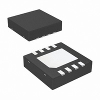
LMV112SD/NOPB National Semiconductor, LMV112SD/NOPB Datasheet

LMV112SD/NOPB
Specifications of LMV112SD/NOPB
LMV112SD
LMV112SDNOPB
LMV112SDNOPBTR
LMV112SDNOPBTR
LMV112SDTR
Available stocks
Related parts for LMV112SD/NOPB
LMV112SD/NOPB Summary of contents
Page 1
... This device enables superb system operation between the base band and the oscillator signal path while eliminating crosstalk. National Semiconductor’s unique technology and design de- liver accuracy, capacitance and load resistance while in- creasing the drive capability of the device. The low power consumption makes the LMV112 perfect for battery applica- tions ...
Page 2
... Absolute Maximum Ratings If Military/Aerospace specified devices are required, please contact the National Semiconductor Sales Office/ Distributors for availability and specifications. + − Supply Voltages (V – ESD Tolerance (Note 2) Human Body Machine Model Storage Temperature Range Junction Temperature (Note 3) 2.7V Electrical Characteristics Unless otherwise specified, all limits are guaranteed for T pF kΩ ...
Page 3
Electrical Characteristics Unless otherwise specified, all limits are guaranteed for T pF kΩ nF. Boldface limits apply at temperature range extremes of operating condition. See (Note 4) L COUPLING Symbol Parameter V Output ...
Page 4
Electrical Characteristics Unless otherwise specified, all limits are guaranteed for T pF kΩ nF. Boldface limits apply at temperature range extremes of operating condition. See (Note 4) L COUPLING Symbol Parameter Miscellaneous Performance ...
Page 5
Block Diagram Pin Description Pin No. Pin Name ENABLE OUT 2 7 OUT 1 8 ENABLE 1 Connection Diagram Ordering Information Package Part Number LMV112SD 8-Pin LLP No Pull Back LMV112SDX V Voltage ...
Page 6
Typical Performance Characteristics pF kΩ and nF, unless otherwise specified. L COUPLING Frequency Response Frequency Response Over Temperature Phase Response Over Temperature www.national.com T = 25˚ 2.7V Phase Response ...
Page 7
Typical Performance Characteristics pF kΩ and nF, unless otherwise specified. (Continued) L COUPLING Full Power Bandwidth Voltage Noise Crosstalk Rejection vs. Frequency T = 25˚ 2.7V Gain Flatness 0.1 ...
Page 8
Typical Performance Characteristics pF kΩ and nF, unless otherwise specified. (Continued) L COUPLING Transient Response Negative Small Signal Pulse Response Large Signal Pulse Response www.national.com T = 25˚ 2.7V ...
Page 9
Typical Performance Characteristics pF kΩ and nF, unless otherwise specified. (Continued) L COUPLING I vs. V SUPPLY SUPPLY PSRR vs. Frequency R vs. Frequency OUT T = 25˚ 2.7V ...
Page 10
Typical Performance Characteristics pF kΩ and nF, unless otherwise specified. (Continued) L COUPLING V vs. I (Sourcing) OUT OUT V vs. I (Sinking) OUT OUT I Sourcing vs. V over Temperature SC SUPPLY www.national.com ...
Page 11
Typical Performance Characteristics pF kΩ and nF, unless otherwise specified. (Continued) L COUPLING SUPPLY ENABLE T = 25˚ 2.7V SUPPLY 20135347 11 = 0V, Enable ...
Page 12
Application Section GENERAL The LMV112 is designed to minimize the effects of spurious signals from the base band chip to the oscillator. Also the influence of varying load resistance and capacitance to the oscillator is minimized, while the drive capability ...
Page 13
Application Section (Continued) LAYOUT DESIGN RECOMMENDATION Careful consideration for circuitry design and PCB layout will eliminate problems and will optimize the performance of the LMV112 best to have the same ground plane on the PCB for all power ...
Page 14
... BANNED SUBSTANCE COMPLIANCE National Semiconductor manufactures products and uses packing materials that meet the provisions of the Customer Products Stewardship Specification (CSP-9-111C2) and the Banned Substances and Materials of Interest Specification (CSP-9-111S2) and contain no ‘‘Banned Substances’’ as defined in CSP-9-111S2. ...


