SY89202UMG Micrel Inc, SY89202UMG Datasheet - Page 4
SY89202UMG
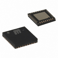
Manufacturer Part Number
SY89202UMG
Description
IC BUFFER/CLK DIVIDER 1:8 32-MLF
Manufacturer
Micrel Inc
Type
Fanout Buffer (Distribution), Divider, Multiplexerr
Series
Precision Edge®r
Datasheet
1.SY89202UMG.pdf
(13 pages)
Specifications of SY89202UMG
Number Of Circuits
1
Ratio - Input:output
1:8
Differential - Input:output
Yes/Yes
Input
CML, LVDS, PECL
Output
LVPECL
Frequency - Max
1.5GHz
Voltage - Supply
2.375 V ~ 3.6 V
Operating Temperature
-40°C ~ 85°C
Mounting Type
Surface Mount
Package / Case
32-MLF®, QFN
Frequency-max
1.5GHz
Number Of Clock Inputs
1
Mode Of Operation
Differential
Output Logic Level
LVPECL
Operating Supply Voltage (min)
2.375V
Operating Supply Voltage (typ)
2.5/3.3V
Operating Supply Voltage (max)
3.6V
Package Type
MLF
Operating Temp Range
-40C to 85C
Operating Temperature Classification
Industrial
Signal Type
CML/LVDS/PECL
Mounting
Surface Mount
Pin Count
32
Lead Free Status / RoHS Status
Lead free / RoHS Compliant
Other names
576-1537-5
SY89202UMG
SY89202UMG
Available stocks
Company
Part Number
Manufacturer
Quantity
Price
Company:

Part Number:
SY89202UMG
Manufacturer:
MICREL
Quantity:
330


Pin Description
Truth Table
Micrel, Inc.
August 2007
Notes:
1. /MR asynchronously forces Q0 – Q7 LOW (/Q0 - /Q7 HIGH).
2. EN forces Q0 – Q7 LOW between 2 and 6 input clock cycles after the falling edge of EN. Refer to “Timing Diagram” section.
3. EN synchronously enables the outputs between 2 and 6 input clock cycles after the rising edge of EN. Refer to “Timing Diagram” section.
10, 19, 22, 31
Pin Number
16, 15, 14,
30, 29, 28,
27, 26, 25,
13, 12, 11
1, 20, 21
/MR
2, 7, 8
24, 23
18, 17
3, 6
0
1
1
1
32
4
5
9
( 1)
/Q1, Q2, /Q2,
Exposed Pad
Q4, /Q4, Q5,
/Q5, Q6, /Q6
Q0, /Q0, Q1,
EN
Pin Name
VREF-AC
DIVSEL1
DIVSEL2
DIVSEL3
Q3, /Q3
Q7, /Q7
IN, /IN
X
GND,
0
1
1
( 2, 3)
VCC
/MR
VT
EN
DIVSEL1
Pin Function
Single-Ended Inputs: These TTL/CMOS inputs select the divide ratio for each of the three
banks of outputs. Note that each of these inputs is internally connected to a 25k Ω pull - up
resistor and will default to logic HIGH state if left open. The input-switching threshold is V
Differential Input: This input pair is the differential signal input to the device. This input accepts
AC- or DC-coupled signals as small as 100mV. The input pair internally terminates to a VT pin
through 50Ω. Note that these inputs will default to an indeterminate state if left open. Please
refer to the “Input Interface Applications” section for more details.
Input Termination Center-Tap: Each side of the differential input pair terminates to the VT pin.
The VT pin provides a center-tap to a termination network for maximum interface flexibility.
See “Input Interface Applications” section for more details.
Reference Voltage: This output biases to V
/IN. For AC-coupled applications, connect V
low ESR capacitor to V
Single-Ended Input: This TTL/CMOS input disables and enables the Q0 – Q7 outputs. This
input is internally connected to a 25kΩ pull-up resistor and will default to logic HIGH state if left
open. The input-switching threshold is V
description, refer to “Timing Diagram” section.
Positive power supply. Bypass with 0.1µF||0.01µF low ESR capacitors as close to VCC pins
as possible.
Bank 2 LVPECL differential output pairs controlled by DIVSEL2: LOW, Q4 – Q6 = ÷2, HIGH,
Q4 – Q6 = ÷4. Unused output pairs may be left open. Each output is designed to drive 800mV
into 50Ω terminated at V
Bank 1 LVPECL differential output pairs controlled by DIVSEL1: LOW, Q0 – Q3 = ÷1, HIGH,
Q0 – Q3 = ÷2. Unused output pairs may be left open. Each output is designed to drive 800mV
into 50Ω terminated at V
Bank 3 LVPECL differential output pair controlled by DIVSEL3: LOW, Q7 = ÷2, HIGH, Q7 =
÷4. Unused output pairs may be left open. Each output is designed to drive 800mV into 50 Ω
terminated at V
Single-Ended Input: This TTL/CMOS-compatible master reset function asynchronously sets
Q0 – Q7 outputs LOW and /Q0 – /Q7 outputs HIGH, and holds them in that state as long as
the /MR input remains LOW. This input is internally connected to a 25k Ω pull - up resistor and
will default to a logic HIGH state if left open. The input-switching threshold is V
Ground: Ground pin and exposed pad must be connected to the same ground plane.
X
X
0
1
DIVSEL2
X
X
0
1
CC
–2V.
CC
CC
CC
DIVSEL3
.
–2V.
–2V.
X
X
0
1
4
CC
Q0 – Q3
/2. For the input enable and disable functional
CC
REF-AC
˜1
˜2
0
0
–1.2V. It is used for AC-coupling inputs IN and
directly to the VT pin. Bypass with 0.01µF
hbwhelp@micrel.com
Q4 – Q6
˜2
˜4
0
0
or (408) 955-1690
M9999-083107-C
CC
/2.
Q7
SY89202U
˜2
˜4
0
0
CC
/2.
Related parts for SY89202UMG
Image
Part Number
Description
Manufacturer
Datasheet
Request
R

Part Number:
Description:
3.3V 800MHz Ultrasmall Dual LVTTL-to-LVPECL Translator (I Temp, Green)
Manufacturer:
Micrel Inc
Datasheet:

Part Number:
Description:
IC XPOINT SW 4X4 PREC 44-MLF
Manufacturer:
Micrel Inc
Datasheet:
Part Number:
Description:
IC XPOINT SWITCH 3.2GBPS 44-MLF
Manufacturer:
Micrel Inc
Datasheet:
Part Number:
Description:
IC XPOINT SWITCH 3.2GBPS 44-MLF
Manufacturer:
Micrel Inc
Datasheet:
Part Number:
Description:
IC XPOINT SWITCH 4X4 LVDS 44-MLF
Manufacturer:
Micrel Inc
Datasheet:
Part Number:
Description:
IC XPOINT SWITCH 4X4 LVDS 44-MLF
Manufacturer:
Micrel Inc
Datasheet:

Part Number:
Description:
IC MUX 2:1 LVPECL DIFF 16MLF
Manufacturer:
Micrel Inc
Datasheet:
Part Number:
Description:
IC MUX 2:1 LVPECL RPE/FSI 16MLF
Manufacturer:
Micrel Inc
Datasheet:
Part Number:
Description:
IC MUX 2:1 LVDS RPE 16-MLF
Manufacturer:
Micrel Inc
Datasheet:
Part Number:
Description:
IC MUX 8:1 PREC LP 44-MLF
Manufacturer:
Micrel Inc
Datasheet:

Part Number:
Description:
IC MUX 2:1 LVDC DUAL 3.3V 32MLF
Manufacturer:
Micrel Inc
Datasheet:
Part Number:
Description:
IC MUX 4:1 LVDS DIFF 2.5V 32MLF
Manufacturer:
Micrel Inc
Datasheet:
Part Number:
Description:
IC MUX 4:1 LVDS DIFF 3.3V 32MLF
Manufacturer:
Micrel Inc
Datasheet:
Part Number:
Description:
IC MUX 4:1 LVDS DIFF 2.5V 32MLF
Manufacturer:
Micrel Inc
Datasheet:
Part Number:
Description:
IC MUX 4:1 LVDS DIFF 3.3V 32MLF
Manufacturer:
Micrel Inc
Datasheet: