CY2DP814ZXC Cypress Semiconductor Corp, CY2DP814ZXC Datasheet - Page 5
CY2DP814ZXC
Manufacturer Part Number
CY2DP814ZXC
Description
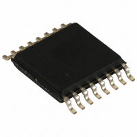
IC CLK FANOUT BUFFER 1:4 16TSSOP
Manufacturer
Cypress Semiconductor Corp
Type
Fanout Buffer (Distribution)r
Datasheet
1.CY2DP814ZXI.pdf
(10 pages)
Specifications of CY2DP814ZXC
Package / Case
16-TSSOP
Number Of Circuits
1
Ratio - Input:output
1:4
Differential - Input:output
Yes/Yes
Input
LVDS, LVPECL, LVTTL
Output
LVPECL
Frequency - Max
450MHz
Voltage - Supply
3.135 V ~ 3.465 V
Operating Temperature
0°C ~ 70°C
Mounting Type
Surface Mount
Frequency-max
450MHz
Number Of Outputs
8
Max Input Freq
450 MHz
Supply Voltage (max)
3.465 V
Supply Voltage (min)
3.135 V
Maximum Power Dissipation
750 mW
Maximum Operating Temperature
+ 70 C
Minimum Operating Temperature
0 C
Mounting Style
SMD/SMT
Lead Free Status / RoHS Status
Lead free / RoHS Compliant
Lead Free Status / RoHS Status
Lead free / RoHS Compliant, Lead free / RoHS Compliant
Available stocks
Company
Part Number
Manufacturer
Quantity
Price
Company:

Part Number:
CY2DP814ZXC
Manufacturer:
SONY
Quantity:
7 825
Part Number:
CY2DP814ZXC
Manufacturer:
CYPRESS/赛普拉斯
Quantity:
20 000


Table 10. High-frequency Parametrics
Notes
Document Number: 38-07060 Rev. *G
Fmax
Fmax(20)
TW
3. RL = 50 ohm ± 1%; Zline = 50 ohm 6 = Ó.
4. CL includes instrumentation and fixture capacitance within 6 mm of the UT.
5. TPA and B are used for prop delay and rise/fall measurements. T
6. When measuring Tr/Tf, tpd, V
7. LVCMOS/LVTTL single-ended input value. Ground either input: when on the B side, non-inversion takes place. If A side is grounded, the signal becomes the complement
Parameter
of the input on B side. See
Figure 3. Differential Receiver to Driver Propagation Delay and Driver Transition Time
Maximum Frequency
V
Maximum Frequency
V
Minimum Pulse
V
DD
DD
DD
= 3.3V
= 3.3V
= 3.3V
Description
Table
OD
G enera tor
point T
3.
P ulse
E n2
E n1
PC
V 1A
V 1B
V 0Y
V 0Z
is held at V
Device concept
B
A
1 . 2 V C M
1 . 2 V C M
50% Duty Cycle tW(50–50)
Standard Load Circuit
20% Duty Cycle tW(20–80)
LVPECL Input
Vin = V
Vout = V
Vin = V
Vout = V
LVPECL Input
VDD
DD
Figure 2. Differential PECL Output
– 2.0V.
T
IH
IH
P L H
OH
OH
V 0 Y -
(Max.)/V
(Max.)/V
V 0 Z
(Min.)/V
(Min.)/V
PC
150
150
S tan dard T erm in ation
T
is used for V
P H L
IL
IL
Conditions
(Min.)
OL
(Min.) F = 100 MHz
OL
G N D
Q
Q
(Max.).(Limit)
(Max.) (Limit)
R
t
OC
measurements only and otherwise connected to V
User Defined
F
VTT & RTT
t
0 V D if f e r e n t ia l
0 V D if f e r e n t ia l
10pF
0 V D if f e r e n t ia l
1.4 V
1.0 V
1.4 V
1.0 V
8 0 %
2 0 %
VDD - 2V
T PA
T P C
T PB
50
50
Min
900
V D D -2V
Typ
[3, 4, 5, 6, 7]
DD
– 2.
Max
450
175
CY2DP814
Page 5 of 10
MHz
MHz
Unit
ps
[+] Feedback
[+] Feedback
Related parts for CY2DP814ZXC
Image
Part Number
Description
Manufacturer
Datasheet
Request
R

Part Number:
Description:
Manufacturer:
Cypress Semiconductor Corp
Datasheet:
Part Number:
Description:
Manufacturer:
Cypress Semiconductor Corp
Datasheet:
Part Number:
Description:
Manufacturer:
Cypress Semiconductor Corp
Datasheet:
Part Number:
Description:
Manufacturer:
Cypress Semiconductor Corp
Datasheet:
Part Number:
Description:
Manufacturer:
Cypress Semiconductor Corp
Datasheet: