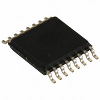
CY2DP814ZXC Cypress Semiconductor Corp, CY2DP814ZXC Datasheet

CY2DP814ZXC
Specifications of CY2DP814ZXC
Available stocks
Related parts for CY2DP814ZXC
CY2DP814ZXC Summary of contents
Page 1
... Commercial temperature range ■ Available in TSSOP package ■ Logic Block Diagram Cypress Semiconductor Corporation Document Number: 38-07060 Rev. *G 1:4 Clock Fanout Buffer Description The Cypress CY2 series of network circuits are produced using advanced 0.35-micron CMOS technology, achieving the industry’s fastest logic. ...
Page 2
Pin Configuration Pin Description Pin Number Pin Name 6, 7 IN+, IN– 2 CONFIG 1, 8 EN1, EN2 16, 15, 14, 13, 12, 11, 10, 9 Q1A, Q1B, Q2A, Q2B, Q3A, Q3B, Q4A, Q4B GND ...
Page 3
Maximum Ratings [1, 2] Storage Temperature: ................................. –65°C to +150°C Ambient Temperature: ........................................ 0°C to 70°C Supply Voltage to Ground Potential (Inputs and V only) .......................................–0.3V to 4.6V CC Table 1. EN1 EN2 Function Table Enable Logic EN1 EN2 H ...
Page 4
Table 6. DC Electrical Characteristics: 3.3V–LVPECL Input Parameter Description V Differential Input Voltage p VCM Common-mode Voltage I Input High Current IH I Input Low Current IL I Input High Current I Table 7. DC Electrical Characteristics: ...
Page 5
Device concept Table 10. High-frequency Parametrics Parameter Description Fmax Maximum Frequency V = 3.3V DD Fmax(20) Maximum Frequency Minimum Pulse V = 3.3V DD Figure 3. Differential Receiver to Driver Propagation Delay and Driver Transition ...
Page 6
Figure 4. Test Circuit and Voltage Definitions for the Driver Common-mode Output Voltage Figure 5. Test Circuit and Voltage Definitions ...
Page 7
... GND InConfig LVTTL/LVCMOS 1 Ordering Information Part Number Pb free CY2DP814ZXC CY2DP814ZXCT Notes 8. V measurement requires equipment with a 3-dB bandwidth of at least 300 MHz All input pulses are supplied by a frequency generator with the following characteristics: t Document Number: 38-07060 Rev. *G VOC Parallel Termination ...
Page 8
Package Drawing and Dimensions Figure 9. 16-Pin TSSOP 4.40 mm Body Z16.173 Note 10. LVPECL or LVDS differential input value. Document Number: 38-07060 Rev. *G CY2DP814 51-85091 *C Page [+] Feedback [+] Feedback ...
Page 9
Document History Page Document Title: CY2DP814 1:4 Clock Fanout Buffer Document Number: 38-07060 Submission REV. ECN No. Date ** 10785 06/07/01 *A 115610 07/02/02 *B 122746 12/15/02 *C 382376 See ECN *D 403374 See ECN *E 2595534 10/23/08 *F 2904795 ...
Page 10
... Cypress against all charges. Any Source Code (software and/or firmware) is owned by Cypress Semiconductor Corporation (Cypress) and is protected by and subject to worldwide patent protection (United States and foreign), United States copyright laws and international treaty provisions. Cypress hereby grants to licensee a personal, non-exclusive, non-transferable license to copy, use, modify, create derivative works of, and compile the Cypress Source Code and derivative works for the sole purpose of creating custom software and or firmware in support of licensee product to be used only in conjunction with a Cypress integrated circuit as specified in the applicable agreement ...


