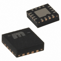
SY89873LMG Micrel Inc, SY89873LMG Datasheet - Page 5

SY89873LMG
Manufacturer Part Number
SY89873LMG
Description
IC CLK DVDR ANY DIFF-LVDS 16MLF
Manufacturer
Micrel Inc
Series
Precision Edge®r
Type
Fanout Buffer (Distribution), Dividerr
Datasheet
1.SY89873LMG.pdf
(11 pages)
Specifications of SY89873LMG
Number Of Circuits
1
Ratio - Input:output
1:3
Differential - Input:output
Yes/Yes
Input
CML, HSTL, LVDS, LVPECL
Output
LVDS
Frequency - Max
2GHz
Voltage - Supply
2.97 V ~ 3.63 V
Operating Temperature
-40°C ~ 85°C
Mounting Type
Surface Mount
Package / Case
16-MLF®, QFN
Frequency-max
2GHz
Function
Clock Divider
Operating Temperature (max)
85C
Operating Temperature (min)
-40C
Package Type
MLF
Pin Count
16
Mounting
Surface Mount
Lead Free Status / RoHS Status
Lead free / RoHS Compliant
Other names
576-1436
Available stocks
Company
Part Number
Manufacturer
Quantity
Price
Company:
Part Number:
SY89873LMG
Manufacturer:
MICREL
Quantity:
436
Part Number:
SY89873LMG
Manufacturer:
MICREL/麦瑞
Quantity:
20 000
Micrel, Inc.
V
Symbol
f
t
t
t
T
t
Notes:
13. Measured with 400mV input signal, 50% duty cycle. All outputs terminated with 100Ω between Q and /Q, unless otherwise stated.
14. Bank A (pass-through) maximum frequency is limited by the output stage. Bank B (input-to-output ÷2, ÷4, ÷8, ÷16) can accept an input frequency >3GHz,
15. Skew is measured between outputs under identical transitions.
16. See “Timing Diagram.”
17. Cycle-to-cycle jitter definition: the variation in period between adjacent cycles over a random sample of adjacent cycle pairs. T
18. Total jitter definition: with an ideal clock input, of frequency ≤ f
M9999-082407
hbwhelp@micrel.com or (408) 955-1690
MAX
PD
SKEW
rr
r
, t
CC
jitter
AC ELECTRICAL CHARACTERISTICS
f
while Bank A will be slew-rate limited.
is the time between rising edges of the output signal.
the specified peak-to-peak jitter value.
= 3.3V ±10%; T
Parameter
Maximum Output Toggle Frequency
(Bank A and Bank B)
Maximum Input Frequency
Differential Propagation Delay
(IN-to-Q)
Within-Device Skew (diff.)
(QB0-to-QB1)
Within-Device Skew (diff.)
(Bank A-to-Bank B)
Part-to-Part Skew (diff.)
Reset Recovery Time
Cycle-to-Cycle Jitter
Total Jitter
Rise / Fall Time (20% to 80%)
A
= –40°C to +85°C; Unless otherwise stated.
Condition
Output Swing: ≥ 200mV
Note 14
Input Swing < 400mV
Input Swing ≥ 400mV
Note 15
Note 15
Note 15
Note 16
Note 17
Note 18
(13)
MAX
(device), no more than one output edge in 10
5
12
output edges will deviate by more than
Min
550
500
600
2.0
3.2
60
Typ
660
610
110
12
7
jitter_cc
Precision Edge
=T
Max
800
750
250
190
n
15
30
10
1
–T
n+1
SY89873L
, where T
ps
Units
ps
GHz
GHz
ps
ps
ps
ps
ps
ps
ps
RMS
PP
®


